Controller
The 8051 — The Moment It Wakes Up
How the classic MCS-51 transitions from cold silicon and hardware reset into executing its very first instruction.
Controller8051MicrocontrollerResetArchitectureStartupProgram CounterHardwareBoot
1. The Machine is Silent
Across our exploration of the classic 8051 architecture, we have observed the machine from almost every perspective. We have inspected its registers and internal memory, watched its timers count machine cycles, traced its hardware interrupts, observed its serial transceiver shift bytes onto physical pins, and seen how assembly instructions directly control internal buses.
Yet underneath all of these systems lies a quiet, fundamental question:
What happens before the first instruction executes?
In our broader journey through computing systems, we investigated how modern processors bridge the gulf from power application to application code in The First Instruction. That exploration traced the extensive, multi-stage choreography of modern boot pipelines—power rail stabilization, brownout supervisory circuits, phase-locked loop clock generation, secure boot chains, bootloaders, and C runtime initialization before handing control to main().
The classic Intel MCS-51 / 8051 offers an extraordinary contrast.
It does not possess a multi-megabyte bootloader, an encrypted secure enclave, or an operating system searching for a filesystem. Its startup path is direct, physical, and hardwired into the silicon itself.
Before the first instruction executes, the silicon is already present. The firmware is stored in non-volatile program memory. The flip-flops of the registers are powered. But the processor has not yet taken a single step.
How does this silent machine actually begin? What physical conditions must be satisfied before the 8051 can fetch byte 0000H from program memory?
2. The Clock Must Exist
Before a single flip-flop can change state predictably, the 8051 requires a steady heartbeat.
The classic 8051 possesses two dedicated pins—XTAL1 and XTAL2—connected to an on-chip inverting amplifier. When an external quartz crystal and two stabilizing capacitors are wired between these pins, the amplifier oscillates at the crystal's resonant frequency.
┌───────────────────────┐
┌───────────┤ XTAL1 │
│ │ │
┌─┴─┐ │ Inverting │ Internal
│ │ Crystal │ Amplifier │ Timing
└─┬─┘ │ Oscillator │ Generator
│ │ │ │
├───────────┤ XTAL2 │ │
│ └───────────────────────┘ │
▼ ▼
12 MHz Pulses ─────────────────────────► ÷12 Divider ──► 1 Machine Cycle (1 µs)
The oscillator does not "start the program." It provides the fundamental periodic pulses that drive the CPU's internal state machine.
In the classic Intel 8051 architecture, timing is structured into three hierarchical layers:
* Oscillator Period (T_OSC): The duration of one crystal clock cycle. For a classic 12 MHz crystal:
T_OSC = 1 / 12 MHz ≈ 83.33 ns
* State (S): One state consists of two oscillator periods (P1 and P2).
* Machine Cycle: One classic 8051 machine cycle consists of 6 sequential states (S1 through S6), which equals 12 oscillator periods:
1 Machine Cycle = 12 × T_OSC = 12 × 83.33 ns = 1.0 µs
Note on Clock Frequencies & Derivatives: While 12 MHz is a classic textbook frequency yielding a convenient 1.0 µs machine cycle, the 8051 can run on various crystal frequencies (such as 11.0592 MHz for accurate serial baud rates). Furthermore, modern high-speed 8051 derivatives often implement single-clock (1T) or two-clock (2T) cores that execute instructions in far fewer oscillator periods. However, on the classic MCS-51, twelve crystal pulses form the bedrock of every single machine cycle.
Without this steady clock pulse, the internal state generator cannot advance from state S1 to S6. The machine remains motionless.
3. Reset is Not an Instruction
A common misconception among programmers accustomed to high-level operating systems is that "reset" is a special function or instruction that the processor executes.
On the classic 8051, reset is entirely electrical.
The 8051 features an active-HIGH hardware input pin: RST (Pin 9).
+5V
│
┌─┴─┐
│ C │ Capacitor (e.g. 10 µF)
└─┬─┘
│
├──────────────────────► RST (Pin 9)
│
┌─┴─┐
│ R │ Resistor (e.g. 8.2 kΩ)
└─┬─┘
│
GND
When power is first applied, the uncharged capacitor acts as a momentary short circuit to +5V, pulling the RST pin HIGH. As current flows through the resistor to ground, the capacitor gradually charges, causing the voltage on the RST pin to decay toward zero.
For a valid reset to occur on a classic 8051, the hardware imposes an explicit timing rule:
The RST pin must remain at a logic HIGH level for a minimum of two complete machine cycles (24 oscillator periods) while the clock oscillator is running.
Why must it remain high for two full cycles?
Because the 8051 samples the RST pin synchronously during phase 2 of state 5 (S5P2) of each machine cycle. The internal reset circuitry requires the first cycle to reliably latch the reset condition and the second cycle to propagate hardware override signals across the internal execution buses, clearing flip-flops and forcing registers into their hardware default states.
Reset is not software. It is a physical override signal seizing control of the silicon.
4. What Reset Actually Does
While the RST pin is held HIGH, what is the processor actually doing?
The answer is: normal instruction execution is completely suspended.
While RST is asserted:
* The Arithmetic Logic Unit (ALU) is idle.
* Normal instruction fetch sequences from program memory are blocked.
* The internal bus lines are held in predetermined electrical states.
* Program counter increment logic is disabled.
Yet, an essential architectural distinction must be made:
Resetting the processor does NOT erase program memory.
The firmware stored inside the on-chip ROM, EPROM, or Flash remains completely intact. The physical bits etched into mask ROM or trapped as floating-gate charges in Flash memory do not vanish when RST goes HIGH. Reset merely forces the processor's active control logic, pointers, and peripheral registers into a known, predictable starting baseline.
5. The Machine Remembers Its Starting State
When the RST pin is held HIGH for the required duration, the internal reset circuitry forces every major register in the CPU and Special Function Register (SFR) space into an exact hardware default value.
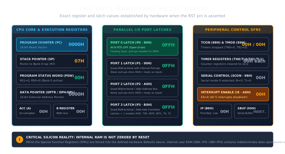
The 8051 Hardware Reset State
Here are the precise classic 8051 reset values established across the silicon:
| Register / Unit |
Reset Value |
Architectural Significance |
| Program Counter (PC) |
0000H |
Execution will commence from program memory address 0000H. |
| Stack Pointer (SP) |
07H |
Stack starts at internal RAM address 07H (top of Register Bank 0). |
| Program Status Word (PSW) |
00H |
All flags cleared; RS1=0, RS0=0 selects Register Bank 0. |
| Data Pointer (DPTR) |
0000H |
Both DPH and DPL are cleared to 00H. |
| Accumulator (ACC / A) |
00H |
Working math register is cleared. |
| B Register |
00H |
Math auxiliary register is cleared. |
| Port Latches (P0, P1, P2, P3) |
0FFH |
All port latch flip-flops are set to 1. |
| Timer Control (TCON) |
00H |
Timers stopped (TR0=0, TR1=0); overflow/interrupt flags cleared. |
| Timer Mode (TMOD) |
00H |
Both timers configured for Mode 0 (13-bit) software gate control. |
| Timer Registers (TH0, TL0, TH1, TL1) |
00H |
Counter registers cleared to zero. |
| Serial Control (SCON) |
00H |
Serial Mode 0 selected; receiver disabled (REN=0); flags TI=0, RI=0. |
| Interrupt Enable (IE) |
00H |
Global interrupt flag cleared (EA=0); all five interrupts disabled. |
| Interrupt Priority (IP) |
00H |
All interrupt sources assigned to low priority. |
| Serial Buffer (SBUF) |
Indeterminate |
Contains random or prior data; not defined on reset. |
A Critical Silicon Reality — Internal RAM is NOT Cleared by Reset:
Notice what is absent from this table: the 128 bytes of general-purpose internal user RAM (08H through 7FH). The 8051 hardware reset does not wipe user RAM. On cold power-up, RAM flip-flops power on in random, indeterminate states (a mix of 1s and 0s determined by microscopic transistor mismatches). On a warm reset (pressing a reset button while powered), internal RAM retains its previous values. Software must explicitly clear RAM if clean memory is required.
6. Why Does SP Start at 07H?
One of the most revealing details in the table above is the Stack Pointer's starting value:
SP = 07H
Why 07H? Why not 00H?
To understand this, we must reconnect to the internal structure mapped in The 8051 Memory Map.
The lowest 32 bytes of 8051 internal RAM (00H through 1FH) are reserved for four switchable Register Banks:
* Bank 0: 00H – 07H (Registers R0 through R7)
* Bank 1: 08H – 0FH
* Bank 2: 10H – 17H
* Bank 3: 18H – 1FH
00H ┌──────────────┐ ◄── R0 (Bank 0)
│ │
07H ├──────────────┤ ◄── R7 (Bank 0) ◄── SP Reset Value (07H)
08H ├──────────────┤ ◄── First Stack Push Lands Here! (R0 of Bank 1)
│ │
1FH ├──────────────┤ ◄── End of Register Banks
20H ├──────────────┤ ◄── Bit-Addressable RAM
│ │
7FH └──────────────┘ ◄── Top of 128-byte Internal Data RAM
The 8051's stack operates with a pre-increment push and post-decrement pop mechanism:
1. When a byte is pushed (via PUSH, LCALL, ACALL, or during an interrupt), the 8051 first increments SP by 1, and then writes the byte into internal RAM at address @SP.
2. When a byte is popped (via POP or RET), the 8051 reads the byte at @SP, and then decrements SP by 1.
Because SP resets to 07H, the very first PUSH or subroutine call will increment SP to 08H before writing data. This ensures that the stack automatically grows upward starting at address 08H—immediately above Register Bank 0.
However, notice what lives at 08H: Register Bank 1!
If your program uses Register Bank 1, or if deep subroutine nesting pushes the stack past 1FH into the bit-addressable RAM area (20H–2FH), the stack will silently corrupt your variables.
This is why virtually every classic 8051 startup sequence begins by explicitly relocating the Stack Pointer to an unused RAM location:
MOV SP, #60H ; Relocate stack well clear of register banks and bit RAM
7. Why Does PSW = 00H Matter?
At reset, the Program Status Word is forced to 00H:
PSW = 00H → CY=0, AC=0, F0=0, RS1=0, RS0=0, OV=0, P=0
The critical bits here are RS1 (Bit 4) and RS0 (Bit 3)—the Register Bank select bits:
RS1:RS0 = 00 → Register Bank 0 is active (addresses 00H–07H)
As established in The 8051 — When Software Speaks the Machine’s Language, the register mnemonics R0 through R7 are not fixed physical locations. They are logical aliases that map to one of four 8-byte banks in internal RAM depending on the state of RS1 and RS0.
Because PSW = 00H at reset, any immediate reference to register R0 directly addresses RAM location 00H:
MOV R0, #55H ; Copies 55H into internal RAM address 00H (Bank 0)
Hardware reset guarantees that software begins in a clean, unambiguous state: Register Bank 0 is active, the carry and overflow flags are clear, and arithmetic parity reflects an accumulator containing zero.
8. The Ports Wake Up Too
When RST is asserted, the four parallel I/O port Special Function Registers—P0, P1, P2, and P3—are all forced to 0FFH:
P0 = 0FFH, P1 = 0FFH, P2 = 0FFH, P3 = 0FFH
It is tempting to summarize this by saying: "All port pins become inputs."
However, in The 8051 — Where Software Meets the Pin, we discovered that the physical reality of the classic 8051 port driver is more nuanced:
VCC
│
[R] Internal Weak Pull-up (P1, P2, P3 only)
│
├──────────────────────────────► Physical Pin (P1.x)
│
┌┴┐
───┤ FET Pull-down Driver
└┬┘
│
GND
1. P1, P2, and P3 (Quasi-Bidirectional Ports):
Setting their port latches to 1 turns off the lower NMOS pull-down transistor. The internal weak pull-up resistor pulls the physical pin HIGH to +5V. In this state, the pin can source a weak current (acting as a logic HIGH output), or an external circuit can easily overpower the weak pull-up and pull the pin LOW to GND (allowing the pin to be read as a digital input).
2. P0 (Open-Drain Port):
Port 0 lacks internal pull-up resistors in its general-purpose I/O mode. Setting its latch to 1 turns off its lower pull-down transistor, leaving the pin in a high-impedance, floating state. Unless external pull-up resistors are wired to Port 0, reading the pin will not produce a valid logic HIGH.
3. P3 (Alternate Peripheral Functions):
Because the P3 latch flip-flops reset to 1, its alternate input functions—such as RXD (Serial Receive), INT0 and INT1 (External Interrupts), and T0/T1 (Timer external inputs)—are unblocked and ready to receive external signals from the board.
Even before the processor fetches its first instruction, the physical boundary between silicon and the circuit board has already been placed into a safe, electrically stable state.
9. Reset is Released
The capacitor on the RST pin charges up, the current decays, and the voltage drops below the 8051's input threshold voltage (V_IL ≈ 0.8 V).
RST transitions from HIGH to LOW.
The processor is released from reset.
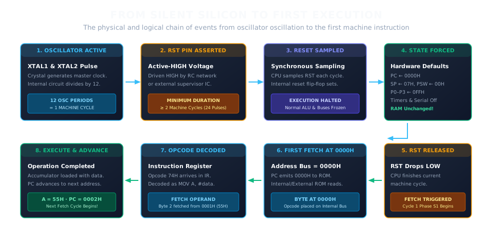
From Silent Silicon to First Execution
Does instruction execution burst forth at the nanosecond RST falls?
No. The 8051 is a strictly synchronous machine.
When RST falls, the CPU's internal clock generator waits until the completion of the current machine cycle. At the start of the very next machine cycle (at State S1, Phase 1), the internal reset override lines release their clamp.
The CPU state counter advances. The execution pipeline engages. The address bus lines are energized.
And the first machine cycle of normal execution begins.
10. The Program Counter Opens the Door
As the internal clamp releases, the CPU must answer one question:
Where do I fetch my first instruction?
In a modern desktop computer, the CPU starts in a specialized execution mode, runs firmware routines from motherboard flash, scans PCI buses, reads disk partition tables, and launches an operating system bootloader.
The classic 8051 does none of this:
* It does not scan memory for code.
* It does not inspect a header or magic byte.
* It does not search for a function named main().
* It does not parse a filesystem.
The hardware reset established only one starting address:
PC = 0000H
┌──────────────────────┐
│ PROGRAM COUNTER (PC) │ ──► Holds 0000H
└──────────┬───────────┘
│
▼
┌──────────────────────┐
│ PROGRAM MEMORY (ROM) │ ──► Location 0000H contains the FIRST BYTE
└──────────────────────┘
The Program Counter is a 16-bit register whose sole function is to present the address of the next byte to be fetched from program memory. Because reset forced PC to 0000H, the very first program memory access must originate at address 0000H.
This address—0000H—is the Reset Vector of the 8051.
Contrast with ARM Cortex-M Vector Tables:
In modern ARM Cortex-M microcontrollers, address 0x00000000 contains the Initial Main Stack Pointer (MSP) value, and address 0x00000004 contains a 32-bit pointer to the Reset Handler function. The ARM processor reads these pointers into registers before executing code.
The classic 8051 has no such pointer table. Address 0000H does not contain an address pointer. Address 0000H contains the actual first executable machine instruction opcode!
11. Where Does the First Byte Come From?
When the 8051 places 0000H onto its internal address bus, where does the physical byte come from?
The answer depends on a single physical pin on the 8051 package: EA (External Access Enable, Pin 31).
+5V (VCC)
│
├──► EA Pin (Pin 31) ──► Fetch 0000H from INTERNAL ROM / Flash
│
GND
│
└──► EA Pin (Pin 31) ──► Fetch 0000H from EXTERNAL ROM via Bus
1. If EA is tied to VCC (HIGH):
The 8051 fetches instructions for addresses 0000H through 0FFFH (the first 4 KB) directly from its internal on-chip ROM or Flash memory. The fetch occurs entirely within the silicon die over internal buses.
2. If EA is tied to GND (LOW):
The 8051 completely ignores internal ROM. It activates its external memory bus, emitting the lower address byte on Port 0, the upper address byte on Port 2, pulsing ALE (Address Latch Enable) to demultiplex the address, and asserting PSEN (Program Store Enable) to read the byte from an external EPROM chip.
In typical self-contained 8051 microcontroller boards, EA is tied HIGH to VCC.
Therefore, address 0000H points directly into the on-chip program ROM holding your compiled firmware.
12. The First Fetch
Now comes the pivotal moment in the life of the machine: the first instruction fetch cycle.
Suppose our program memory contains the following two bytes starting at address 0000H:
Address: 0000H 0001H
Memory: [ 74H ] [ 55H ]
As we learned in the Assembly exploration, the byte 74H is the machine code opcode for MOV A, #data, and 55H is the immediate numerical data.
Let us trace the physical cycle across the silicon:
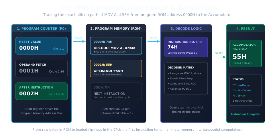
The First Instruction Fetch & Execution
Phase 1: Fetching the Opcode (State S1 to S4)
1. Address Assertion: The Program Counter outputs 0000H onto the internal program address bus.
2. ROM Read: Internal read control strobes the program memory array at cell 0000H.
3. Byte Transfer: The memory cell releases the byte 74H onto the internal data bus.
4. Instruction Latching: The byte 74H is latched into the CPU's Instruction Register (IR).
5. PC Increment: The Program Counter automatically increments to 0001H.
Phase 2: Decoding the Opcode
Inside the CPU, the Instruction Decoder matrix evaluates the bit pattern 74H (01110100b). It recognizes this pattern as:
* An operation targeting the Accumulator.
* An addressing mode of Immediate Data.
* An instruction length of 2 bytes.
* An execution duration of 1 machine cycle.
Phase 3: Fetching the Operand (State S5 to S6)
Because the decoder recognized a 2-byte instruction, the timing generator triggers a second read cycle within the same machine cycle:
1. PC (0001H) addresses program memory.
2. The byte 55H is placed onto the internal data bus.
3. The CPU routing logic directs this byte straight to the input latches of the Accumulator.
4. PC increments to 0002H.
Phase 4: Execution
At the closing edge of State S6, the Accumulator latches the data.
ACC = 55H (01010101b)
The instruction is finished. Exactly one microsecond has elapsed since reset released.
The machine has executed its very first instruction.
13. What Does ORG 0000H Really Mean?
Now we can appreciate the connection between assembly source code and hardware reality.
When writing 8051 assembly, the very first line of code almost universally reads:
ORG 0000H
MOV A, #55H
What is ORG?
ORG stands for Origin. It is an assembler directive (or pseudo-instruction).
It is not an 8051 machine instruction. It does not produce an opcode. It never enters the Instruction Register, and the 8051 CPU never executes it.
Instead, ORG 0000H is an instruction to the assembler program running on your computer:
“Take the machine code bytes generated by the instructions that follow, and place them starting at address 0000H in the resulting binary ROM image.”
The assembler obeys the directive and places 74H at ROM address 0000H and 55H at 0001H.
When the 8051 is powered on, hardware forces PC = 0000H. The CPU reads 0000H and encounters the exact bytes placed there by the ORG 0000H directive.
ORG 0000H is the structural handshake between human software tools and the silicon reset vector.
14. What If the First Instruction is a Jump?
While placing MOV A, #55H at 0000H demonstrates the fetch cycle cleanly, no serious 8051 embedded program puts application code directly at 0000H.
Why?
Because of what lies immediately ahead in program memory: The Interrupt Vector Table.
As we discovered in The 8051 — When Hardware Decides to Interrupt, the 8051's five hardware interrupt vectors are located at fixed, permanent addresses in low program memory:
Address Space:
0000H ──► Reset Vector (Execution starts here)
0001H ──┐
0002H ──┴── Only 3 BYTES available before the first interrupt!
0003H ──► External Interrupt 0 (IE0) Vector
000BH ──► Timer 0 Overflow (TF0) Vector
0013H ──► External Interrupt 1 (IE1) Vector
001BH ──► Timer 1 Overflow (TF1) Vector
0023H ──► Serial Port (RI / TI) Vector
0030H ──► First Safe Free Space for Main Firmware Code
Look at the distance between the Reset Vector (0000H) and External Interrupt 0 (0003H):
Available Space = 0003H - 0000H = 3 Bytes!
If you write four bytes of instructions at 0000H, your startup code will spill directly into the interrupt handler for External Interrupt 0! If that interrupt triggers, the CPU will jump directly into the middle of your code.
For this reason, the first instruction of virtually every 8051 program is an unconditional jump:
ORG 0000H
LJMP START ; Long Jump: 3-byte instruction (Opcode: 02H [High] [Low])
ORG 0003H
; External Interrupt 0 Service Routine (ISR)
RETI
; ... Other Interrupt Vectors ...
ORG 0030H
START:
; Real application initialization begins here, safely beyond the vectors!
MOV SP, #60H
Notice the elegance of this architectural design:
1. LJMP (Long Jump) is an instruction that takes exactly 3 bytes:
* Byte 1: Opcode (02H)
* Byte 2: Target address high byte (00H)
* Byte 3: Target address low byte (30H)
2. It occupies addresses 0000H, 0001H, and 0002H—filling the gap before 0003H perfectly.
3. When the 8051 wakes up, its very first instruction tells it: "Immediately jump over the interrupt vector table to address 0030H."
The Program Counter loads 0030H, and application initialization begins safely away from the interrupt vectors.
15. The First Few Instructions
Now let us examine what a real, robust 8051 startup sequence actually does during its first microseconds of life:
ORG 0000H
LJMP START ; 1. Jump over interrupt vectors
ORG 0030H
START:
MOV SP, #60H ; 2. Relocate Stack Pointer above register banks & bit RAM
MOV P1, #00H ; 3. Clear Port 1 outputs to drive connected LEDs LOW
MOV TMOD, #01H ; 4. Configure Timer 0 in Mode 1 (16-bit Timer)
MOV TH0, #0D8H ; 5. Load Timer 0 high byte for 10 ms delay
MOV TL0, #0F0H ; 6. Load Timer 0 low byte
SETB TR0 ; 7. Start Timer 0 counting machine cycles
SETB ET0 ; 8. Enable Timer 0 Interrupt
SETB EA ; 9. Enable Global Interrupts
MAIN_LOOP:
SJMP MAIN_LOOP ; 10. Idle here; timers and interrupts take over
Observe how this compact sequence of instructions takes ownership of the raw silicon:
1. MOV SP, #60H (Stack Initialization):
Overcomes the default reset value of 07H, moving the stack to safe RAM (60H–7FH) so subroutine calls will not overwrite Register Bank 1 or bit-addressable memory.
2. MOV P1, #00H (Port Configuration):
Overcomes the default reset value of 0FFH, driving Port 1 pins LOW to establish a known state for external hardware actuators.
3. MOV TMOD, #01H & SETB TR0 (Peripheral Activation):
Transitions Timer 0 from its disabled reset state (TR0=0) into active counting mode, transforming crystal clock pulses into timed software events.
4. SETB EA (Interrupt Activation):
Overcomes the global reset disable (EA=0), opening the gate for hardware interrupts to service real-time events.
In less than ten machine cycles, software has transformed a generic, reset-state silicon chip into a dedicated embedded control system.
16. What is NOT Happening?
When engineers trained on modern platforms study classic microcontrollers, they often carry mental models from modern computing that do not apply to the classic 8051.
To understand the 8051 deeply, we must be explicit about what is NOT happening:
* There is no BIOS or UEFI: The 8051 does not execute a system BIOS stored in a separate chip to discover hardware.
* There is no Operating System Boot: No Linux kernel, RTOS, or monitor program loads unless you explicitly write one into your program ROM.
* There is no Automatic Search for main(): The C compiler simply arranges for its runtime initialization code (CRT0.A51) to be located at 0000H. When that code finishes setting up the stack and clearing variables, it executes a jump to the symbol _main. The silicon itself knows nothing about C or main().
* There is no Filesystem: Program memory is a flat, linear, 16-bit address space. There are no directories, files, or partition headers.
* No Flash-to-RAM Code Relocation: On classic microcontrollers, code is executed directly in place out of non-volatile Program ROM (Execute-in-Place / XIP). The CPU does not copy firmware into internal RAM before running it; internal RAM is far too small (only 128 bytes!).
* Reset Does Not Zero Internal RAM: Any variable initialization (such as setting uninitialized global variables in C's .bss section to zero) must be performed by software startup loops. The hardware leaves internal RAM values untouched across reset.
The classic 8051's wake-up mechanism is pure, unfiltered determinism: Power on → RST asserted → Registers forced → RST released → Fetch from 0000H.
17. The Complete Wake-Up Sequence
We can now assemble the complete chronological architecture of the 8051 waking up, from external electrical power to running firmware:
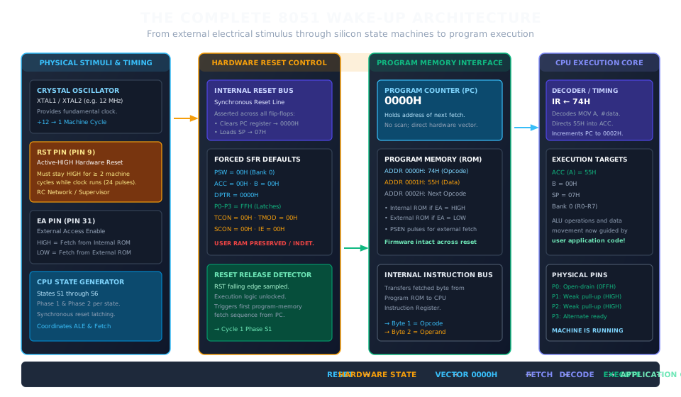
The Complete 8051 Wake-Up Architecture
The sequence unfolds in five distinct, immutable phases:
1. Phase 1: Clock Stabilization
* Crystal circuit energizes; XTAL1 and XTAL2 stabilize into steady oscillation.
* Internal divide-by-12 circuit establishes machine cycle states (S1–S6).
2. Phase 2: Hardware Reset Clamping
* Active-HIGH voltage on RST pin sampled during state S5P2.
* Held HIGH for at least 2 machine cycles (24 clock pulses).
* Internal reset lines assert; normal instruction execution halted.
3. Phase 3: Hardware State Establishment
* PC forced to 0000H.
* SP forced to 07H.
* PSW forced to 00H (Register Bank 0 selected).
* Port latches P0–P3 forced to 0FFH.
* Peripherals disabled: TCON = 00H, TMOD = 00H, SCON = 00H, IE = 00H.
* Internal data RAM remains unmodified.
4. Phase 4: Reset Release & Synchronization
* RST drops below threshold (V_IL < 0.8 V).
* CPU completes current machine cycle and releases internal clamps at next S1P1.
5. Phase 5: First Instruction Execution
* PC outputs 0000H onto program memory address bus.
* Internal ROM (or external via EA) delivers opcode to Instruction Register.
* Instruction Decoder configures internal data paths.
* CPU executes first instruction and advances PC.
18. The Machine is Awake
The 8051 does not "launch" an application.
It simply exists in an unbroken continuum of physical states:
RESET ──► STATE ──► VECTOR ──► FETCH ──► DECODE ──► EXECUTE
Hardware reset establishes the machine's initial baseline. The Program Counter supplies the first address. Program memory yields the stored binary bytes. The instruction decoder translates those bits into electrical gating signals. And the execution core changes the state of internal flip-flops.
From that first machine cycle onward, the controller is no longer waking up. It is running.
All the subsystems we have explored across the 8051 architecture—its memory map, its register banks, its timer overflows, its interrupt vectors, its serial shift buffers, and its physical I/O pins—were already there, etched in silicon, waiting in total stillness.
The first instruction is the singular moment when software begins to move through the machine.
Yet notice what we quietly assumed throughout this journey.
We traced the path:
PC = 0000H
│
▼
Program Memory
│
▼
First Opcode
We know the address.
We know the byte.
We know how the central processing unit decoded and executed it.
But what, exactly, answered when the 8051 asked for address 0000H?
The first instruction was already waiting.
Somewhere.
And the moment the processor took its first digital breath, that quiet assumption became a much deeper question.
Because knowing where the 8051 looks is not the same as knowing what answers.
Current Exploration
The 8051 — The Moment It Wakes Up