Controller
The 8051 — When the Controller Looks Beyond Itself
How the classic MCS-51 coordinates multiplexed buses, transparent latches, and hardware strobes to connect with external memory.
Controller8051MicrocontrollerExternal MemoryBusALEPSENMOVXHardware Architecture
1. The Question We Left Behind
In The 8051 — The Moment It Wakes Up, we followed the classic 8051 through its earliest moments of life.
We saw electrical power stabilize, watched the crystal oscillator establish its rhythmic 12-pulse machine cycle, and observed the hardware reset line release the CPU core into its defined initial state. From address 0000H, the Program Counter stepped forward:
PC = 0000H ──► Fetch Opcode ──► Decode ──► Execute
Yet that exploration closed with an unanswered question:
Where did that byte actually come from?
In self-contained embedded systems, the answer is simple: the byte is etched directly inside the chip's on-die ROM or Flash. But the classic Intel MCS-51 architecture was designed with a far more ambitious capability. It does not have to keep its thoughts confined within its own silicon.
What happens when an instruction is not stored inside the 8051? What happens when firmware outgrows the chip, or when an application needs tens of thousands of bytes of data storage that the silicon die cannot provide?
To answer this, we must examine what occurs when the controller reaches beyond its physical package.
2. Inside is Not Always Enough
To understand why the 8051 looks beyond itself, we must return to the internal boundaries mapped in The 8051 Memory Map.
The standard classic Intel 8051 provides:
* 4 Kilobytes of on-chip Program Memory (ROM / EPROM).
* 128 Bytes of on-chip Data Memory (RAM).
For simple appliance controllers, 4 KB of code and 128 bytes of scratchpad memory were sufficient. But as systems expanded to manage complex industrial machinery, communications buffers, and instrumentation displays, these internal limits became a wall.
Yet, inside the 8051 CPU core, the registers were already designed for a much larger universe:
* The Program Counter (PC) is 16 bits wide. A 16-bit register can address:
2^16 = 65,536 bytes (64 Kilobytes of Program Memory)
* The Data Pointer (DPTR) is also 16 bits wide. It can address:
2^16 = 65,536 bytes (64 Kilobytes of External Data Memory)
Here lies the fundamental architectural duality of the 8051: Harvard Architecture.
┌──────────────────────────────────┐ ┌──────────────────────────────────┐
│ PROGRAM MEMORY (CODE) │ │ DATA MEMORY (XDATA) │
│ Up to 64 KB │ │ Up to 64 KB │
│ • Holds instructions & tables │ │ • Holds variables & buffers │
│ • Read-only access by the CPU │ │ • Read/write access by the CPU │
│ • Controlled by PSEN strobe │ │ • Controlled by RD and WR │
└──────────────────────────────────┘ └──────────────────────────────────┘
The 8051 maintains two distinct 64-kilobyte address spaces: one for code, and one for external data.
The silicon core knows how to generate 16-bit addresses for both. But if those memories live on separate physical chips outside the 8051 package, how does a 40-pin microcontroller physically reach them?
3. A 16-Bit Address Needs 16 Bits
To access an external memory chip, the CPU must deliver a 16-bit binary address to the memory chip's address pins (A0 through A15).
Sixteen address bits require sixteen physical pins on the microcontroller package. Furthermore, an 8-bit computer must transfer 8 bits of data into or out of the memory chip, requiring another 8 physical pins (D0 through D7).
If the 8051 dedicated separate pins for every signal:
* 16 pins for Address (A0–A15)
* 8 pins for Data (D0–D7)
* Power, Ground, Oscillator, Reset, and Control pins
The chip would have required a massive, expensive package with far more than 40 pins. In 1980, packaging costs were a major fraction of total silicon cost.
Intel's architects solved this through a disciplined division of labor across the parallel ports:
16-bit Address
│
┌─────────┴─────────┐
▼ ▼
High Address (A15–A8) Low Address (A7–A0)
│ │
Port 2 Port 0
(Pins 21–28) (Pins 32–39)
│
AD0–AD7
(Address AND Data!)
* Port 2 (Pins 21–28): Emits the High Address Byte (A8 through A15). These pins remain dedicated to high address lines throughout the external memory access cycle.
* Port 0 (Pins 32–39): Emits the Low Address Byte (A0 through A7). But Port 0 does not stop there. It is also the port that must transmit and receive the 8-bit data byte!
Because Port 0 carries both address and data, it is designated as AD0–AD7.
However, Port 0 cannot carry the low address byte and the data byte at the same physical instant. It must carry them sequentially: address first, then data.
This brings us to one of the most critical concepts in microcomputer hardware: time-multiplexing.
4. How Can One Pin Carry Two Different Things?
How can a single physical pin on Port 0 represent an address bit at one moment and a data bit a few nanoseconds later without confusing the memory chip?
The memory chip requires the complete 16-bit address to remain perfectly stable while data is being read or written. If Port 0 changed from address to data while the memory chip was still decoding the address, the memory would read from the wrong location.
The solution is an external hardware memory element: an Octal Transparent Latch (typically the industry-standard 74HC373 or 74LS373).
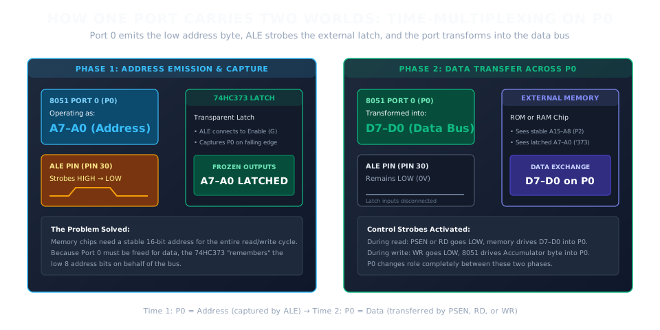
How One Port Carries Two Worlds: Time-Multiplexing on P0
The coordination between Port 0 and the external latch relies on a dedicated strobe pin: ALE (Address Latch Enable, Pin 30).
Here is the exact choreography:
Phase 1: Address Emission & Latch Capture
1. At the beginning of the memory cycle, the 8051 places the low address byte (A0–A7) onto Port 0, and the high address byte (A8–A15) onto Port 2.
2. The 8051 asserts the ALE pin HIGH. This opens the transparent inputs of the external 74HC373 latch.
3. The 8051 drives ALE LOW. On this falling edge, the 74HC373 instantly freezes and latches the state of Port 0.
4. The outputs of the 74HC373 now present a steady, permanent A0–A7 to the external memory chips for the remainder of the cycle.
Phase 2: Data Transfer
1. Having safely stored the low address inside the 74HC373, the 8051 disconnects its address drivers from Port 0.
2. Port 0 is now completely free to act as the 8-bit bidirectional Data Bus (D0–D7).
3. If reading, external memory drives data onto Port 0; if writing, the 8051 drives data onto Port 0.
Through this brief pulse on ALE, eight physical pins on the microcontroller do the work of sixteen.
Connection to GPIO: As we discovered in The 8051 — Where Software Meets the Pin, Port 0 behaves as an open-drain port when used as general-purpose I/O. But during external memory access, internal control hardware connects Port 0's upper pull-up FETs directly to the internal address and data buses. During bus cycles, Port 0 operates as a high-speed, active push-pull bus driver.
5. The Pins That Make the Bus
When the 8051 looks outside, seven distinct functional groups of pins form the external memory interface:
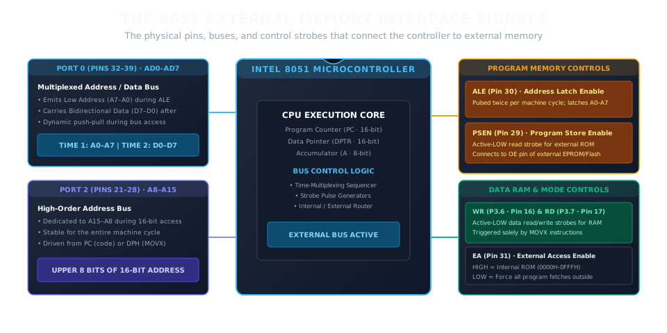
The 8051 External Memory Interface Signals
| Pin / Port |
Signal Name |
Direction |
Physical Role in External Memory Access |
| Port 0 (32–39) |
AD0–AD7 |
Bidirectional |
Time-multiplexed low address byte (A0–A7) followed by data byte (D0–D7). |
| Port 2 (21–28) |
A8–A15 |
Output |
Dedicated high address byte for 16-bit external memory operations. |
| Pin 30 |
ALE |
Output |
Address Latch Enable: Pulses to strobe the low address into an external 74HC373 latch. |
| Pin 29 |
PSEN |
Output |
Program Store Enable: Active-LOW read strobe for external Program ROM. |
| Pin 16 (P3.6) |
WR |
Output |
External Data Write: Active-LOW strobe commanding external RAM to store data. |
| Pin 17 (P3.7) |
RD |
Output |
External Data Read: Active-LOW strobe commanding external RAM to output data. |
| Pin 31 |
EA |
Input |
External Access Enable: Selects whether low program memory is internal or external. |
Notice the roles of P3.6 (WR) and P3.7 (RD).
In the GPIO exploration, we noted that Port 3 was special because every pin carried an alternate hardware function. Now we see why: P3.6 and P3.7 are not merely digital outputs; they are the physical read and write control lines of the external memory bus.
6. One Bus, Two Different Memories
A common point of confusion is how the 8051 connects to two completely different 64-kilobyte memory spaces (Program ROM and Data RAM) over the very same address lines (A0–A15) and data lines (D0–D7).
If address 2000H in Program ROM contains an opcode, and address 2000H in external RAM contains a sensor reading, how does the system prevent them from colliding on the bus?
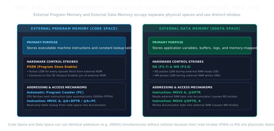
One Bus, Two Memories: Harvard Architecture Outside the Die
The answer lies in the control strobes:
| Dimension |
External Program Memory |
External Data Memory |
| Address Space |
0000H – FFFFH (64 KB Code) |
0000H – FFFFH (64 KB XDATA) |
| Primary Chip Type |
EPROM, EEPROM, Flash ROM |
Static RAM (SRAM), Memory-Mapped I/O |
| Read Control Strobe |
PSEN (Program Store Enable) |
RD (Port 3.7) |
| Write Control Strobe |
None (Program memory is read-only) |
WR (Port 3.6) |
| CPU Instruction |
Opcode fetch (automatic) or MOVC |
MOVX A, @DPTR or MOVX @DPTR, A |
| Connected Pin |
Connects to ROM OE (Output Enable) |
Connects to RAM OE and WE |
Because PSEN and RD are entirely separate physical pins on the 8051, the external ROM and external RAM are never enabled at the same time:
* When fetching instructions, the 8051 pulses PSEN LOW. The ROM turns on its outputs, while the RAM remains completely silent.
* When executing a data read (MOVX), the 8051 pulses RD LOW. The RAM turns on its outputs, while the ROM remains completely silent.
The two memory systems share the copper traces of the address and data buses, but they answer to completely different masters.
7. When the CPU Reads an Instruction from Outside
Now we can trace the exact physical sequence when the 8051 fetches an opcode from external Program Memory:
Program Counter (PC)
│
▼ (16-bit address generated)
┌────────┴────────┐
▼ ▼
Port 2 Port 0
(A15–A8) (A7–A0)
│ │
│ ▼
│ ALE pulses HIGH → LOW
│ │
│ ▼
│ 74HC373 Latch captures A7–A0
│ │
└────────┬────────┘
▼
Full 16-bit Address (A0–A15) stable at External ROM
│
▼
PSEN pulses LOW (Pin 29)
│
▼
External ROM places Opcode onto Port 0 (D7–D0)
│
▼
8051 latches Opcode into Instruction Register (IR)
│
▼
Decode & Execute
Observe the profound realization here:
The instruction fetch is no longer an abstract idea occurring inside silicon flip-flops.
The Program Counter places a binary number onto internal buses. Internal multiplexers route that number to Port 0 and Port 2. Transistors switch on physical pins. Copper traces on the circuit board charge to +5V and 0V. The external latch snaps shut on ALE's falling edge. The PSEN line pulls down. A completely separate silicon chip on the PCB senses the strobe, reads its own memory matrix, and drives eight bits of charge back across the board into Port 0.
The opcode has physically traveled through the world to reach the processor's Instruction Register.
8. When the CPU Reads and Writes External Data
External data memory is not accessed automatically by the Program Counter. It is accessed deliberately by software using a dedicated assembly instruction: MOVX (Move External).
The 8051 provides two primary addressing modes for external RAM:
1. 16-Bit Addressing via the Data Pointer (DPTR)
When software needs to access anywhere within the full 64 KB external RAM space, it loads the 16-bit address into DPTR:
MOV DPTR, #2000H ; Load 16-bit address into DPTR (DPH=20H, DPL=00H)
MOVX A, @DPTR ; Read byte from external RAM address 2000H into A
To write data into external RAM:
MOV DPTR, #2000H ; Target address
MOV A, #55H ; Data to write
MOVX @DPTR, A ; Write byte 55H into external RAM address 2000H
2. 8-Bit Paged Addressing via Registers R0 or R1
The 8051 also provides an 8-bit external access mode:
MOV R0, #80H ; Load 8-bit address into R0
MOVX A, @R0 ; Read external RAM byte at address 80H
In this mode, Port 0 emits the 8-bit address from R0, while Port 2 emits the current contents of the Port 2 SFR latch. This allows external memory to be partitioned into 256-byte pages.
9. Read and Write Become Electrical Events
Let us zoom into the physical pin activity caused by MOVX:
The Anatomy of MOVX A, @DPTR (External Data Read)
1. Address Phase: DPH (20H) appears on Port 2. DPL (00H) appears on Port 0.
2. Latch Strobe: ALE pulses HIGH then falls LOW, capturing 00H in the external 74HC373 latch.
3. Bus Turnaround: Port 0's drivers release, floating the port to receive data.
4. Read Strobe: Pin 17 (P3.7 / RD) transitions LOW.
5. Memory Response: The external SRAM senses RD LOW and drives the byte stored at address 2000H onto Port 0.
6. Data Capture: The 8051 samples Port 0 and copies the bits into the Accumulator.
7. Cycle End: RD returns HIGH, and the SRAM disconnects its drivers.
ALE ──────┐ ┌─────────────────────────────
└──────┘
P0 ──[ A7–A0 ]──────────[ D7–D0 (From RAM) ]──
RD ─────────────────────┐ ┌────────
└────────────┘
The Anatomy of MOVX @DPTR, A (External Data Write)
1. Address Phase: DPH appears on Port 2, DPL appears on Port 0.
2. Latch Strobe: ALE pulses to freeze the low address in the 74HC373.
3. Data Setup: The 8051 immediately drives the Accumulator's byte onto Port 0 (D0–D7).
4. Write Strobe: Pin 16 (P3.6 / WR) pulses LOW.
5. Data Capture: On the rising edge of WR, the external SRAM latches the byte from Port 0 into its internal storage cells.
A single assembly instruction—MOVX—is literally a recipe for an orchestrated sequence of microsecond voltage transitions across half a dozen physical pins.
10. What EA Really Decides
Now we can demystify a pin that appeared during reset: EA (External Access Enable, Pin 31).
When the 8051 powers on, what determines whether it reads address 0000H from internal ROM or external ROM?
The voltage wired to Pin 31:
EA Pin (Pin 31)
│
┌─────────────────┴─────────────────┐
▼ ▼
EA Tied to +5V (VCC) EA Tied to GND
│ │
Addresses 0000H–0FFFH (4 KB) ALL Addresses (0000H–FFFFH)
fetched from INTERNAL ROM fetched from EXTERNAL ROM
│ │
Addresses 1000H–FFFFH (60 KB) │
fetched from EXTERNAL ROM │
│ │
└─────────────────┬─────────────────┘
▼
External Access Enabled
1. If EA is tied to VCC (HIGH):
The 8051 executes from its on-chip 4 KB program memory for addresses 0000H through 0FFFH. If the Program Counter reaches 1000H or higher, the CPU automatically activates PSEN and fetches subsequent instructions from external ROM.
2. If EA is tied to GND (LOW):
The internal ROM is completely disabled and bypassed. The 8051 fetches every single instruction—beginning at reset vector 0000H—from external ROM.
A Crucial Silicon Distinction:
The EA pin controls PROGRAM MEMORY ONLY.
It has nothing to do with external RAM. The MOVX instruction always accesses external RAM regardless of whether EA is tied to VCC or GND. EA answers only one question: "Where do instructions live?"
11. The 8051 Pins Change Their Identity
In The 8051 — Where Software Meets the Pin, we observed the 8051's parallel ports as simple general-purpose digital I/O lines.
Now we witness their true architectural versatility:
Normal GPIO Mode External Memory Bus Mode
┌────────────────┐ ┌────────────────────────┐
│ P0.0 – P0.7 │ ──► Dynamic Mode ──►│ AD0 – AD7 (Muxed Bus) │
│ P2.0 – P2.7 │ ──► Dynamic Mode ──►│ A8 – A15 (High Address)│
│ P3.6 (GPIO) │ ──► Alternate ────► │ WR (Memory Write) │
│ P3.7 (GPIO) │ ──► Alternate ────► │ RD (Memory Read) │
│ Pin 30 │ ──────────────────► │ ALE (Latch Strobe) │
│ Pin 29 │ ──────────────────► │ PSEN (ROM Read) │
└────────────────┘ └────────────────────────┘
A pin on a classic microcontroller is not a fixed, single-purpose wire.
When running simple code in internal memory, Port 0 and Port 2 can read switches and drive LEDs. But the moment the Program Counter crosses beyond internal ROM, or the moment the CPU decodes a MOVX instruction, the internal hardware instantly takes over the pins:
* Port 0's open-drain switches disengage and active push-pull bus transceivers take command.
* Port 2 outputs freeze their latch functions and become high-address drivers.
* Port 3 pins 6 and 7 become bus timing strobes.
The physical pins seamlessly change their identity to serve the larger architecture.
12. One Complete External Memory Transaction
Here is the centerpiece of the entire external architecture—the complete hardware schematic connecting the 8051 to an external memory system:
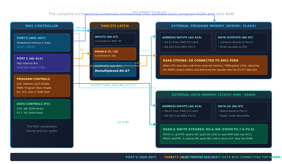
The Complete 8051 External Memory System
Let us follow one complete cycle as the 8051 reads a data byte from external SRAM address 8050H:
1. Instruction Fetch: The CPU decodes MOVX A, @DPTR, where DPTR = 8050H.
2. Address Generation: The CPU asserts 80H on Port 2 and 50H on Port 0.
3. Address Latch Pulse: Pin 30 (ALE) pulses HIGH, then drops LOW. The falling edge triggers the 74HC373 latch, capturing 50H on outputs Q0–Q7.
4. Stable Address Bus: The external SRAM now sees the full 16-bit address:
* Upper bits A8–A15 (80H) from Port 2.
* Lower bits A0–A7 (50H) from the 74HC373 latch.
5. Bus Handover: Port 0 switches from driving address bits to listening for data.
6. Strobe Assertion: Pin 17 (RD) pulses LOW. This connects directly to the SRAM's OE (Output Enable) pin.
7. Data Transfer: The SRAM activates its output buffers, driving the byte stored at cell 8050H onto the Port 0 data bus.
8. CPU Capture: The 8051 latches the byte from Port 0 into the Accumulator.
9. Cycle Termination: RD rises HIGH. The SRAM disconnects its drivers, leaving the bus clear for the next cycle.
Nine distinct micro-events. Three separate silicon chips. One single machine cycle.
13. From Assembly to the Outside World
Throughout this exploration series, we have traced instructions from human intent to physical silicon:
Human Concept
│
▼
Assembly Mnemonic (MOVX A, @DPTR)
│
▼
Machine Code (E0H)
│
▼
Instruction Register & Decoder
│
▼
Internal Bus Timing Sequencer
│
▼
Physical Pin Drivers (Port 0, Port 2, ALE, RD)
│
▼
Copper PCB Traces
│
▼
External Memory Silicon Responds
A single statement in code is ultimately an electrical disturbance traveling through copper and silicon.
Yet Assembly is not the only language that can orchestrate this machine.
In high-level languages like C, a cross-compiler targeting the 8051 compiles variables designated with special storage classes directly into these external memory operations:
// Keil C51 memory-mapped external variable
unsigned char xdata sensor_buffer[256];
void read_sensor(void) {
unsigned char val = sensor_buffer[0]; // Compiles directly to MOVX A, @DPTR!
}
The compiler translates the C array access into an address loaded into DPTR, followed by MOVX A, @DPTR. The syntax is higher-level; the programmer's cognitive burden is lighter. But down at the pins, the physics is identical: ALE pulses, Port 0 multiplexes, the 74HC373 latches, RD pulls low, and electrons flow across the board.
The language changes. The silicon does not.
14. The 8051 Has Reached Beyond Itself
We began our journey into the 8051 at the physical layer—examining how silicon gates form registers, how 128 bytes of RAM are partitioned into working banks, and how special function registers control hardware.
We watched timers count crystal pulses into signals. We saw interrupt lines seize the Program Counter. We observed serial shift registers stream bytes through physical transceivers. We saw how assembly mnemonics translate into machine operations. And we watched the silent machine wake up from reset at address 0000H.
Now, we have seen the controller reach outside its own packaging.
The 8051 began as a tiny rectangle of silicon inside a 40-pin ceramic dual-inline package.
We followed its memory.
We followed its instructions.
We followed its registers.
We followed its signals into pins.
And finally, we followed those pins across circuit board traces into other pieces of silicon.
At some point, the physical boundary of the microcontroller stopped being the boundary of the system.
So perhaps the most profound realization is not where the 8051 ends.
It is:
Where does the 8051 actually become the system?
Current Exploration
The 8051 — When the Controller Looks Beyond Itself
Next →
None