Controller
The 8051 — Where Software Meets the Pin
How the classic 8051 turns port latches, quasi-bidirectional drivers, and open-drain FETs into physical machine control.
Controller8051MicrocontrollerGPIOPortsQuasi-BidirectionalOpen-DrainPush-PullSCONHardware ArchitectureEmbedded Systems
1. Four Doors to the Outside World
In our main-tree exploration The Physical Edge of Software, we discovered the profound transformation that occurs at the boundary of a computing system. Deep within the core, software exists as pure abstraction—numbers shifting between registers, arithmetic comparisons, and logical branches. But at the edge of the silicon die, that mathematical abstraction must become a physical voltage capable of moving electrons through copper wires.
That boundary is General Purpose Input/Output: GPIO.
How did the architects of the classic Intel 8051 implement this boundary in silicon?
If you inspect the 40-pin Dual In-line Package (DIP) of an 8051, thirty-two of its pins belong to four distinct eight-bit input/output ports:
8051 CORE
│
┌─────────────┼─────────────┐
│ │ │
PORT 0 PORT 1 PORT 2 PORT 3
(Pins 32–39) (Pins 1–8) (Pins 21–28) (Pins 10–17)
8 Lines 8 Lines 8 Lines 8 Lines
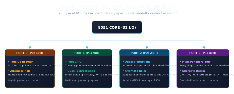
Four Doors to the Outside World
Thirty-two physical lines connecting software to the physical universe.
On a datasheet pinout diagram, they look like four identical eight-bit ports.
They aren't.
In software, you can write an eight-bit number to Port 0, Port 1, Port 2, or Port 3 using the exact same assembly syntax. But underneath the silicon surface, each of these four ports possesses a fundamentally different relationship with the hardware around it. One is an open-drain bus interface; one is pure general-purpose I/O; one multiplexes high memory addresses; and one is a multi-peripheral hardware hub.
To understand how the 8051 touches the physical world, we must look past the pin names and peer into the transistor circuitry behind each door.
2. The Port SFRs
Continuing our journey across the 8051's Special Function Register surface, we meet the four port registers:
PORT REGISTER MEMORY MAP:
├── P0 → Address 80H (Bit-addressable from 80H to 87H)
├── P1 → Address 90H (Bit-addressable from 90H to 97H)
├── P2 → Address A0H (Bit-addressable from A0H to A7H)
└── P3 → Address B0H (Bit-addressable from B0H to B7H)
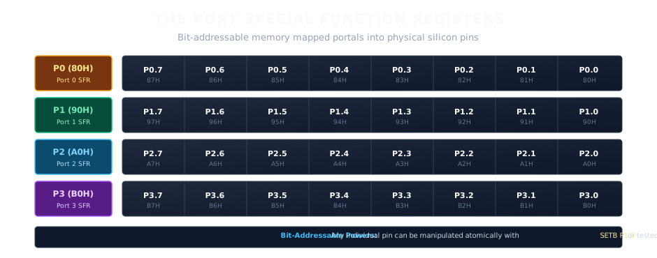
The Port Special Function Registers
Notice that all four port SFRs sit on hexadecimal addresses ending in 0H. As we discovered in The 8051 — Where Software Touches Hardware, this alignment grants all four ports direct bit-addressability.
Software does not have to read an entire eight-bit port, execute an OR mask, and write the byte back just to turn on a single LED. The 8051 can address every individual copper pin directly:
SETB P1.0 ; Drive Pin 1 HIGH (Address 90H)
CLR P1.0 ; Drive Pin 1 LOW
JB P3.2, SENSOR ; Test Pin 12 (P3.2 / INT0) and branch if HIGH
Writing to a port SFR is fundamentally unlike writing to a variable in internal RAM.
When you write to RAM address 30H, an electrical charge settles into a static flip-flop and remains inside the silicon memory array. When you write to P1 (90H), however, the internal write strobe latches the value into an output stage whose transistors directly charge or discharge a piece of copper lead sticking out of the plastic package.
The bit does not remain an idea. It becomes a voltage.
3. What Does a “1” Actually Do?
In modern microcontroller programming, developers are accustomed to a strict mental model: a pin must be configured as either an Output or an Input before it can be used.
In a modern ARM Cortex or AVR microcontroller, setting up a pin requires writing to a dedicated Direction Register (DDR or MODER):
MODERN MCU MENTAL MODEL:
Direction Bit = 1 → Pin is an Output (Push-Pull active drive)
Direction Bit = 0 → Pin is an Input (High-Impedance listening)
The classic 8051 has no Direction Registers.
There is no DDR0, no P1DIR, and no configuration mode register. There is only the port register itself (P0, P1, P2, P3).
How can a single register allow a pin to serve as both an output and an input?
The answer lies in the classic 8051's quasi-bidirectional port architecture:
* When software writes 0 to a port bit:
An internal low-side Field Effect Transistor (FET) turns heavily ON. This provides a direct, low-resistance path to Ground (0V). The pin actively sinks current, pulling the physical voltage down to a solid logic LOW.
* When software writes 1 to a port bit:
The low-side pull-down FET turns completely OFF. The strong path to Ground is released. The pin is pulled up toward +5V through the port's internal pull-up circuitry.
* Because the pull-up is relatively weak:
An external switch or sensor can easily overpower the internal pull-up and pull the pin to Ground without causing a short circuit! If an external sensor drives the line LOW, the pin falls to 0V; if the sensor floats or drives HIGH, the internal pull-up holds the pin at 5V.
Writing a 1 does not merely mean "output a HIGH voltage."
Writing a 1 releases the strong clamp to Ground, allowing the external world to influence the voltage on the pin. Writing a 1 is what turns an 8051 pin into an input.
4. Push-Pull, Open-Drain and Quasi-Bidirectional
To appreciate the elegance—and the limitations—of the 8051's I/O pins, we must examine the three classic driver topologies used in digital electronics:
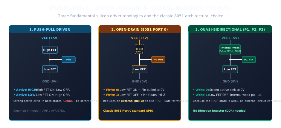
Push-Pull, Open-Drain and Quasi-Bidirectional Topologies
1. The Push-Pull Driver
A push-pull output stage contains two active transistors wired in series between VCC (+5V) and Ground (0V):
* High-Side Transistor (PMOS): Turns ON to connect the pin directly to VCC (actively "pushing" current out).
* Low-Side Transistor (NMOS): Turns ON to connect the pin directly to GND (actively "pulling" current in).
Push-pull drivers are fast and powerful. They switch sharp square waves into capacitive loads.
However, push-pull outputs have a dangerous flaw: they cannot be tied together. If Output A drives HIGH (5V) while Output B on the same wire drives LOW (0V), a near-zero-resistance short circuit forms between VCC and Ground through the two chips, causing destructive current spikes.
2. The Open-Drain Driver
An open-drain output removes the high-side transistor entirely.
It contains only a single low-side transistor connected to Ground:
* To output LOW (0), the transistor turns ON, pulling the pin to 0V.
* To output HIGH (1), the transistor turns OFF, leaving the pin completely disconnected—floating in a high-impedance (Hi-Z) state.
Because an open-drain pin cannot supply voltage on its own, it requires an external pull-up resistor connected between the pin and VCC. Multiple open-drain pins can be safely wired to the same physical trace—creating a "wired-AND" bus (such as I2C) where any chip can pull the line LOW without damage.
3. The Quasi-Bidirectional Driver (8051 P1, P2, P3)
Why did Intel term the 8051's ports quasi-bidirectional (meaning "partially" or "seemingly" bidirectional)?
In a true bidirectional port, control logic dynamically switches the pin between a strong push-pull output driver and a completely disconnected high-impedance input buffer.
In the classic 8051, the pin is permanently connected to both its output driver and its input buffer simultaneously.
Instead of a high-side push-pull transistor, Ports 1, 2, and 3 use an internal pull-up network:
* A very weak pull-up transistor (acting like a ~50 kΩ resistor) that remains on whenever the latch holds a 1, gently holding the pin at 5V while consuming microamps.
* A momentary strong pull-up transistor that fires for only two oscillator clock cycles whenever the latch transitions from 0 to 1. This transient burst rapidly charges line capacitance, speeding up the slow rise time typical of passive pull-ups.
Because the steady-state HIGH drive is weak, an external circuit can ground the pin safely. The pin serves as an input and an output at the exact same physical moment, without needing a direction register.
5. Why P0 Is Different
Now we encounter the famous exception of the 8051 family: Port 0.
If you wire an LED between a Port 1 pin and Ground, write SETB P1.0, and inspect the circuit, the LED lights up (or glows faintly through the internal pull-up).
If you wire the exact same LED between a Port 0 pin and Ground and write SETB P0.0:
Nothing happens. The pin remains completely inert.
Why?
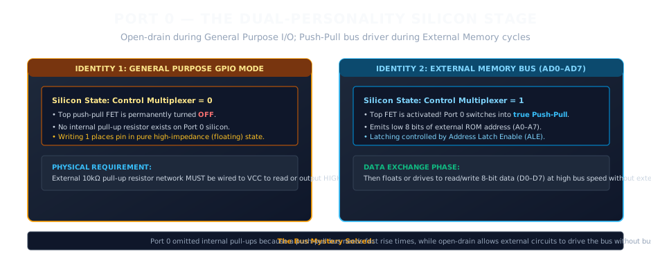
Port 0 Open-Drain and Bus Topologies
Unlike Ports 1, 2, and 3, Port 0 has no internal pull-ups on its silicon die.
When used as general-purpose I/O, Port 0 is a true open-drain port:
* Writing 0 turns ON the low-side NMOS transistor, actively pulling the pin to 0V.
* Writing 1 turns OFF the low-side NMOS transistor, leaving the pin floating in a completely disconnected, high-impedance state!
To use Port 0 as a normal output or input, the hardware engineer must solder an external resistor pack (typically eight 10 kΩ pull-up resistors connected to +5V) to pins 32 through 39.
The Secret Behind the Omission
Why would Intel's engineers omit pull-up resistors on Port 0 while including them on the other three ports?
Because Port 0 has a second identity:
PORT 0 DUAL PERSONALITY:
├── General Purpose I/O → Open-Drain (Requires external pull-ups)
└── External Memory Bus → Multiplexed Address / Data Bus (AD0–AD7)
When used as general-purpose I/O, Port 0 is open-drain and requires external pull-ups to output a logic HIGH.
During external memory access, Port 0 becomes the multiplexed AD0–AD7 address/data bus. Its GPIO open-drain behavior is different from its external-memory bus function. In this bus role, internal control logic switches the pins away from the port latch and connects them directly to the memory interface: Port 0 carries A0–A7 during the address phase and D0–D7 during the data phase.
Intel omitted internal pull-ups because static pull-up resistors would slow down bus transitions and draw unnecessary power during external memory access.
The port we thought was GPIO was engineered from the beginning to be a computer bus.
6. P3 — The Port With Another Identity
If Port 0's alternate identity belongs to memory, Port 3's alternate identity belongs to the peripheral subsystem.
Port 3 (pins 10 through 17) possesses internal pull-ups, functioning as a standard quasi-bidirectional GPIO port. But look closely at the pinout:
PORT 3 ALTERNATE FUNCTIONS:
├── P3.0 → RXD (Serial Data Input)
├── P3.1 → TXD (Serial Data Output)
├── P3.2 → INT0 (External Interrupt 0 Input)
├── P3.3 → INT1 (External Interrupt 1 Input)
├── P3.4 → T0 (Timer 0 External Counter Input)
├── P3.5 → T1 (Timer 1 External Counter Input)
├── P3.6 → WR (External Data Memory Write Strobe)
└── P3.7 → RD (External Data Memory Read Strobe)
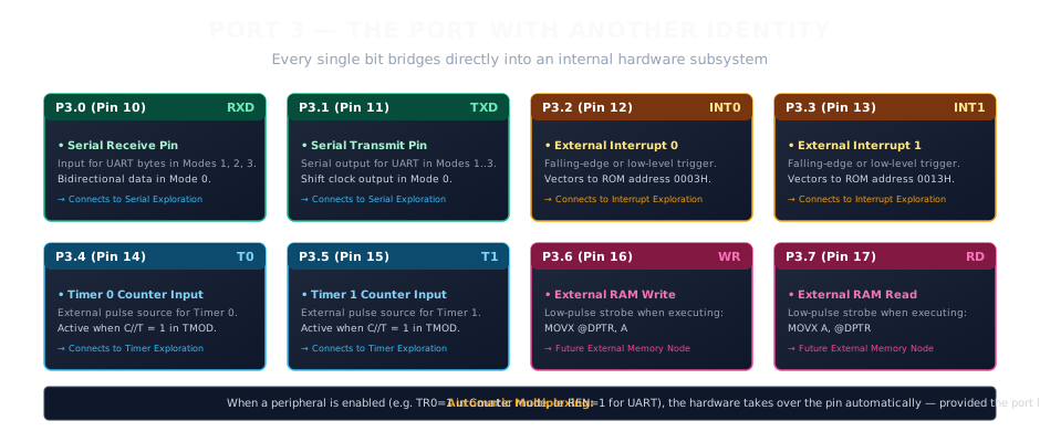
Port 3 Alternate Functions
Every single bit of Port 3 is an entry point into a hardware subsystem we have previously explored:
* In The 8051 — When the Controller Learns to Speak, we watched bytes flow through P3.0 (RXD) and P3.1 (TXD).
* In The 8051 — When Hardware Decides to Interrupt, we watched physical voltage edges on P3.2 (INT0) and P3.3 (INT1) freeze the Program Counter and vector execution into ISRs.
* In The 8051 — Four Shapes of Time, we pulsed P3.4 (T0) and P3.5 (T1) to drive internal counter registers in Counter mode.
* And when we explore external memory, P3.6 (WR) and P3.7 (RD) will supply the timing pulses that command external static RAM chips to capture or emit data.
The Golden Rule of Port 3
How does silicon switch a pin between ordinary GPIO and its alternate hardware function?
Inside Port 3's output circuitry, the internal peripheral signal is routed through a logic gate that combines it with the Port 3 latch bit.
To use an alternate input function (such as RXD, INT0, or T0), software must write a 1 into the corresponding Port 3 latch bit.
Writing a 1 turns off the low-side pull-down transistor, freeing the copper pin so the incoming serial pulses, interrupt triggers, or counter ticks can pass cleanly into the internal peripheral logic.
7. The Pin Is Not the Latch
One of the most subtle concepts in 8051 architecture is the distinction between the Port Latch and the Physical Pin:
CPU INTERNAL BUS
│
▼
PORT D-LATCH ────────> [Stores Software State: Q and /Q]
│
▼
OUTPUT DRIVERS ────────> [FETs & Pull-ups Drive the Voltage]
│
▼
PHYSICAL PIN ────────> [Copper Lead Touched by External Circuits]
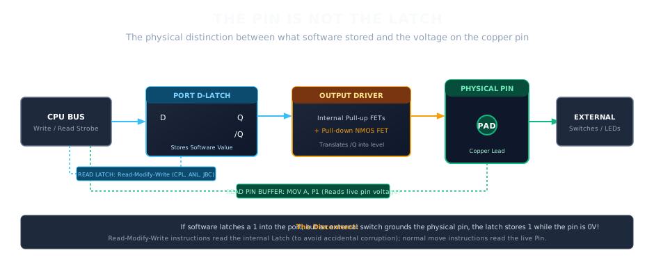
The Pin Is Not the Latch
Consider this physical scenario:
1. Software executes: SETB P1.0 (Writes 1 to Port 1, Bit 0).
2. The internal D-latch stores Q = 1. The low-side pull-down transistor turns OFF.
3. Outside the chip, an operator presses a push-button that connects Pin P1.0 directly to Ground (0V).
What is the state of this port?
* The Port Latch still stores 1.
* The Physical Pin is held at 0V (Logic 0).
The latch and the pin have diverged!
Read-Pin vs. Read-Modify-Write
Because of this divergence, the 8051 CPU contains two distinct internal read buffers:
1. Instructions that Read the Physical Pin:
Instructions such as MOV A, P1 or MOV C, P1.0 read the voltage currently present on the copper pin through an input buffer. If the push-button is pressed, the accumulator reads 0.
2. Instructions that Read the Port Latch (Read-Modify-Write):
Consider what would happen if software executed a complement instruction:
CPL P1.0 ; Invert Bit 0 of Port 1
If CPL read the physical pin (which is grounded to 0 by the user's finger), it would invert 0 into 1, leaving the latch at 1. But more dangerously, if an instruction operated on the whole port:
ANL P1, #0FEH ; Clear Bit 0, leave Bits 1–7 alone
If ANL read the physical pins, any other pin that was currently being pulled LOW by an external circuit would have a 0 read and written back into its internal latch! The software would inadvertently lock those input pins permanently LOW, destroying their configuration!
To prevent this silent catastrophe, Intel designed specific instructions to perform a Read-Modify-Write operation:
* Instructions like CPL, ANL, ORL, XRL, DJNZ, INC, and JBC do not read the physical pin.
* They read the value stored in the internal Port Latch, modify the bits, and write the result back!
The physical pin observes the outside world; the latch preserves the programmer's intent.
8. Why Writing a 1 Makes a Pin an Input
Because this concept is so counterintuitive to programmers arriving from modern platforms, let us isolate its exact electrical mechanics:
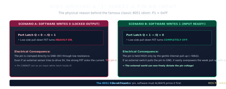
Why Writing 1 Makes a Pin an Input
Suppose an external digital sensor outputs 0V for "idle" and 5V for "active". You connect this sensor to Pin P1.2 of an 8051.
If the Latch holds 0:
* The internal low-side NMOS transistor is saturated ON.
* Pin P1.2 is clamped directly to Ground through a fraction of an ohm.
* When the sensor tries to drive 5V, it collides with the saturated transistor. A heavy current flows, and the pin remains held near 0V.
* The CPU reads P1.2 and sees 0. Even if the sensor pulses 5V, the CPU still reads 0. The pin is electrically locked.
If the Latch holds 1:
* The internal low-side NMOS transistor is cut OFF.
* The pin is connected to +5V only through the weak internal pull-up (~50 kΩ).
* When the sensor outputs 0V, it easily sinks the tiny microamp current through the 50 kΩ resistor, pulling the pin to 0V.
* When the sensor outputs 5V, no current flows, and the pin sits cleanly at 5V.
* The input buffer reads the true, unfiltered state of the external sensor!
This gives rise to the universal 8051 assembly idiom for preparing an input port:
; INITIALIZE PORT 1 AS AN INPUT PORT:
MOV P1, #0FFH ; Write 1s to all eight latches
; READ EXTERNAL SIGNALS:
MOV A, P1 ; Read the live states of all 8 external pins
Writing 0FFH does not force the pins to output 5V against the world's will. It releases all eight low-side clamps, throwing open the doors so the outside world can speak.
9. The 8051's Different Way of Thinking About GPIO
When software engineers transition between microcontroller families, the shift in GPIO philosophy is often jarring:
MODERN GPIO (ARM Cortex / STM32 / ESP32):
├── GPIOx_MODER → Select Input, Output, Alternate, or Analog
├── GPIOx_OTYPER → Select Push-Pull or Open-Drain
├── GPIOx_OSPEEDR → Select Low, Medium, High, or Very High Speed
├── GPIOx_PUPDR → Select No Pull, Pull-Up, or Pull-Down
└── GPIOx_AFR → Multiplex to one of 16 Alternate Functions
CLASSIC 8051 GPIO:
└── Px Register → Write 0 to drive LOW; Write 1 to read INPUT or float HIGH
In modern computing, flexibility is achieved through extensive configuration registers. A single GPIO pin on an STM32 might require configuring four separate 32-bit registers before a single bit can be toggled.
The classic 8051 arrived from an era where silicon area was precious and simplicity was paramount.
Intel's engineers did not burden the chip with direction registers, slew-rate controls, or pull-up selectors. Instead, they built an analog compromise directly into the silicon:
* The quasi-bidirectional driver eliminated the need for direction registers.
* The transient pull-up speed boost eliminated the sluggish rise times of passive pull-ups without requiring full push-pull circuitry.
* The Read-Modify-Write instructions protected latch states from external pin loading without software overhead.
It is not an inferior design; it is a different architectural philosophy. It traded configurable options for immediate, single-instruction operational elegance.
10. The Deeper Realization
When you look at an 8051 memory map, P0, P1, P2, and P3 look like four ordinary Special Function Registers alongside TMOD or SCON.
They aren't.
SOFTWARE INTENT (MOV P1, #55H)
│
▼
PORT SPECIAL FUNCTION REGISTER (90H)
│
▼
STATIC PORT D-LATCHES (Q and /Q)
│
▼
OUTPUT DRIVER TRANSISTORS (Pull-down FETs & Pull-up Network)
│
▼
PHYSICAL COPPER PINS (0V to 5V Electrical Potentials)
│
▼
THE PHYSICAL UNIVERSE (Actuators, Sensors, Relays, Displays)
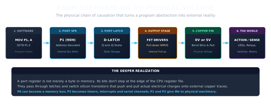
From Software Bit to Physical Voltage
Most CPU registers live in an isolated digital sanctuary. When the accumulator changes from 00H to FFH, nothing moves in the physical world except a few microscopic charges inside the ALU.
A port register breaks that isolation.
Its bits do not stop at the edge of the CPU bus. They continue through silicon latches, steer high-current Field Effect Transistors, cross bond wires, and push electrical current out into copper PCB traces.
And the four doors are uniquely specialized:
* Port 0 sheds its pull-ups to become an open-drain gate for multi-chip buses, ready to morph into high-speed address and data lines.
* Port 1 stands as pure, unencumbered general-purpose I/O.
* Port 2 guards the high-order address space of external memory.
* Port 3 binds the CPU's internal timers, serial channels, and interrupt arbiters directly to the physical world.
Software sets the bits in memory.
Hardware turns them into voltage, current, and physical action.
Current Exploration
The 8051 — Where Software Meets the Pin