Controller
The 8051 Memory Map
How the classic microcontroller organizes program code, internal RAM, register banks, bit-addressable memory, and Special Function Registers into distinct address spaces.
Controller8051MicrocontrollerMemory MapRAMROMSFRArchitectureEmbedded Systems
1. One Controller, Different Kinds of Memory
We now know that the 8051 has program memory and data memory.
We know it contains a central processor, on-chip storage, working registers, physical I/O ports, timers, a serial interface, and an interrupt controller.
But that raises a strange question.
If the CPU needs to access program code, variables, registers, peripherals, and control registers, how does it know where each one lives?
When the processor executes an instruction, how does it know whether an address refers to an instruction byte in firmware, a variable in scratchpad memory, or a hardware pin on the outside of the chip?
The answer begins with a fundamental distinction:
PROGRAM MEMORY ≠ DATA MEMORY
In the 8051, code and data do not share the same address space. They are segregated into separate logical and physical worlds:
8051
│
├── Program Memory → Code / Instructions
│
└── Data Memory → Data / Runtime state / SFR access
This strict architectural separation is known as the Harvard architecture.
Because the address spaces are independent, address 0000H in program memory has nothing to do with address 00H in data memory. They are reached by different internal signals, accessed by different processor instructions, and served by different physical circuits.
Before mapping these regions, we must establish a crucial distinction:
ADDRESS SPACE ≠ PHYSICALLY IMPLEMENTED MEMORY
An address space is the total range of numerical addresses that a processor's address bus or pointer registers are capable of generating. Physically implemented memory, by contrast, is the actual silicon storage cells manufactured inside the chip.
When an engineer says that the 8051 architecture has a 64 KB program address space, it does not mean that the original 8051 chip contains 64 KB of internal ROM.
It means the architecture has the capacity to address up to 64 KB across its lifetime.
Let us see how that space is actually arranged.
2. The Program Memory Map
Program Memory (often called Code Memory) is where the microcontroller's firmware resides. It contains the machine instructions fetched, decoded, and executed by the CPU.
In the 8051 architecture, program addresses are 16-bit wide.
Because a 16-bit binary number can generate 216 = 65,536 unique combinations, the 8051 architecture can address up to 64 KB of program space, spanning from 0000H through FFFFH.
The classic 8051 contains 4 KB of on-chip program ROM.
This factory-masked internal ROM occupies the lowest 4,096 addresses of the space: 0000H through 0FFFH.
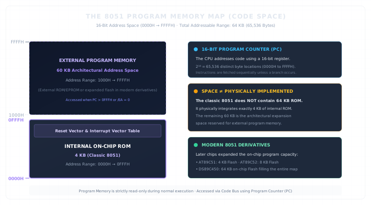
The 8051 Program Memory Map
The classic 8051 program memory map is structured as follows:
0000H ─────────────────
Internal Program ROM
4 KB
0000H–0FFFH
0FFFH ─────────────────
1000H ─────────────────
External Program
Memory region
(architectural address space)
...
FFFFH ─────────────────
When the processor powers up or receives a reset signal, the Program Counter (PC) is forced to 0000H. That is where execution begins.
The very first few bytes of this internal ROM are reserved for critical vectors:
- 0000H: System Reset entry point
- 0003H through 0023H: Interrupt Vector Table (holding jump targets for external interrupts, timers, and the serial port)
Above 0023H, the remainder of the 4 KB internal ROM holds the main program instructions.
If a system requires more than 4 KB of code, the architecture allows up to 60 KB of external program memory to be connected off-chip, spanning from 1000H to FFFFH. The microcontroller automatically begins fetching from external memory as soon as the Program Counter advances beyond 0FFFH.
It is important to remember that this 4 KB on-chip ROM is specific to the classic 8051.
Modern 8051 derivatives and compatible successors do not alter the 16-bit address space, but they frequently expand the amount of internal memory built into the silicon. For example, an Atmel AT89C51 provides 4 KB of reprogrammable Flash, an AT89C52 provides 8 KB of Flash (0000H–1FFFH), and high-performance variants such as the DS89C450 integrate a full 64 KB of on-chip Flash, occupying the entire 0000H–FFFFH map without requiring external chips.
Regardless of the chip derivative, program memory remains dedicated to code. It is read-only at runtime during normal program execution.
3. Data Memory Is Where It Gets Interesting
Program memory is relatively straightforward.
Data memory is where the 8051 becomes much more interesting.
While program memory holds static instructions that do not change during runtime, Data Memory holds the dynamic state of the machine: variables, loop counters, temporary calculation results, hardware status flags, and the execution stack.
In the classic 8051, the primary internal data-address space is addressed by an 8-bit address, giving a total range of 28 = 256 possible addresses: 00H to FFH.
Internal Data Address Space: 00H → FFH (256 Addresses)
However, these 256 addresses are not one monolithic block of storage. They are divided into two completely different architectural zones:
00H–7FH → Internal RAM (128 Bytes)
80H–FFH → Special Function Registers (SFR Address Space)
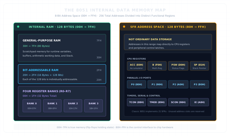
The 8051 Internal Data Memory Map
The lower 128 bytes (00H through 7FH) consist of physical, high-speed static RAM built into the chip. Within these 128 bytes, memory is further partitioned to serve distinct functional roles:
- 00H–07H → Register Bank 0 (8 bytes)
- 08H–0FH → Register Bank 1 (8 bytes)
- 10H–17H → Register Bank 2 (8 bytes)
- 18H–1FH → Register Bank 3 (8 bytes)
- 20H–2FH → Bit-addressable RAM (16 bytes = 128 individually addressable bits)
- 30H–7FH → General-purpose RAM (80 bytes of scratchpad storage and stack)
Above 7FH, spanning from 80H to FFH, lies the Special Function Register (SFR) address space.
This visual and functional boundary is critical.
The lower half (00H–7FH) is true internal memory — storage cells designed to hold data.
The upper half (80H–FFH) is an address space mapped to the control latches and status registers of the processor and its peripherals.
Let us inspect each of these regions in detail.
4. Where Did the Registers Go?
When writing or reading 8051 assembly code, one immediately encounters registers named R0, R1, R2, R3, R4, R5, R6, and R7.
This raises an obvious question:
If R0 through R7 are working registers, where are they?
In many microprocessors, registers are isolated, dedicated physical circuits wired directly inside the execution unit. In the 8051, Intel's designers chose an elegant embedded design:
The working registers are mapped directly into the first 32 bytes of Internal RAM (00H through 1FH).
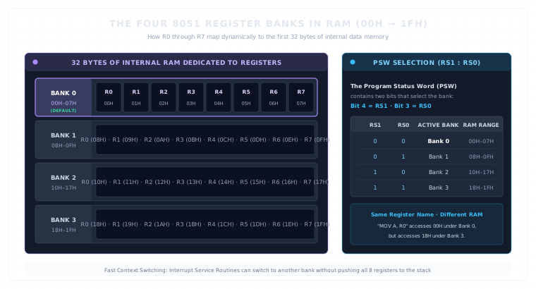
The Four 8051 Register Banks in RAM
Even more interesting, there is not just one set of eight registers. There are four identical register banks, each containing eight bytes:
Register Bank 0:
00H → R0
01H → R1
02H → R2
03H → R3
04H → R4
05H → R5
06H → R6
07H → R7
Register Bank 1:
08H–0FH → R0 through R7
Register Bank 2:
10H–17H → R0 through R7
Register Bank 3:
18H–1FH → R0 through R7
When a program uses R0, it isn't accessing some completely separate memory region.
R0 refers to the R0 location in the currently selected register bank.
How does the CPU know which register bank is active?
It checks two control bits inside the Program Status Word (PSW): bits RS1 (Bit 4) and RS0 (Bit 3).
RS1 RS0 Active Bank RAM Addresses
0 0 Bank 0 00H–07H (Default upon Reset)
0 1 Bank 1 08H–0FH
1 0 Bank 2 10H–17H
1 1 Bank 3 18H–1FH
Upon system reset, RS1 and RS0 default to 00. Therefore, Bank 0 is selected, and instructions like MOV A, R0 read from RAM address 00H.
If the software switches RS1:RS0 to 11, Bank 3 becomes active. The exact same instruction — MOV A, R0 — now automatically reads from RAM address 18H without requiring the programmer to change a single instruction mnemonic.
Why did Intel build four register banks into RAM?
In embedded systems, responsiveness is everything. When an urgent real-time interrupt occurs, a conventional processor must waste dozens of clock cycles pushing R0 through R7 onto the stack to save their contents, and waste dozens more restoring them later.
On the 8051, an interrupt handler can simply change RS1:RS0 to switch to Bank 1. It immediately gets a fresh set of eight working registers without touching the main program's registers and without executing a single stack push. When finished, it restores the bank bits, and the main program resumes instantly.
The registers are not separate from RAM. They are RAM.
5. The Bit-Addressable Area
Directly above the register banks sits one of the most distinctive features of the 8051 architecture:
The Bit-Addressable RAM, located from byte address 20H through 2FH.
20H–2FH → 16 Bytes of Bit-Addressable RAM
Sixteen bytes might seem like a modest amount of memory. But consider the arithmetic:
16 bytes × 8 bits per byte = 128 individually addressable bits.
In this 16-byte window, every single bit has its own unique bit address, numbered sequentially from 00H through 7FH.
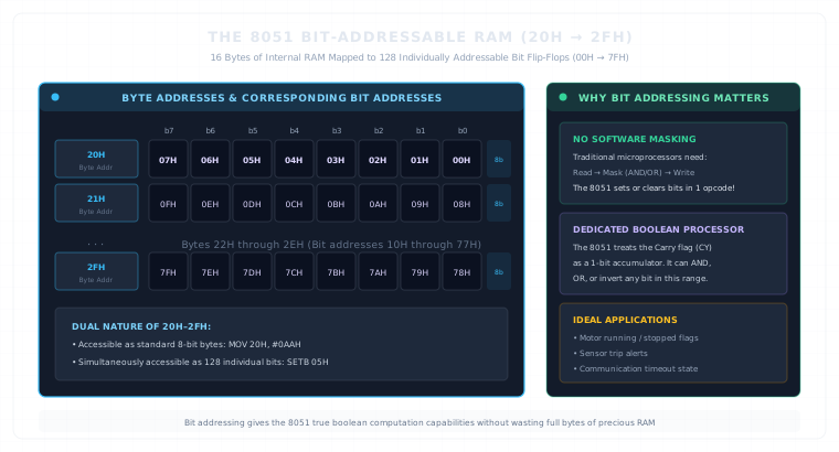
The 8051 Bit-Addressable RAM
The mapping unfolds bit by bit across the 16 bytes:
Byte 20H → Bit addresses 00H through 07H (Bits 0 to 7)
Byte 21H → Bit addresses 08H through 0FH (Bits 0 to 7)
Byte 22H → Bit addresses 10H through 17H (Bits 0 to 7)
...
Byte 2FH → Bit addresses 78H through 7FH (Bits 0 to 7)
This region possesses a dual nature:
You can treat it as normal byte storage. Writing MOV 20H, #0FFH writes an 8-bit byte into RAM address 20H.
Alternatively, you can treat it as 128 independent 1-bit boolean switches.
The 8051 includes instructions specifically engineered to manipulate individual bits:
- SETB 05H — sets bit 05H (which is Bit 5 of byte 20H) to 1.
- CLR 07H — clears bit 07H (Bit 7 of byte 20H) to 0.
- CPL 00H — inverts bit 00H (Bit 0 of byte 20H).
Why does this matter so much in a microcontroller?
In control systems, software constantly tracks single-bit physical states:
- Is the emergency button pressed?
- Has the timer expired?
- Is the motor running?
- Is the sensor calibrated?
In standard microprocessors without bit addressing, modifying a single flag requires three separate operations: reading the whole byte, performing a logical OR or AND mask in an accumulator, and writing the byte back out.
The 8051's dedicated boolean processing capabilities allow a program to set, clear, test, or jump on an individual bit in a single instruction.
Part of the RAM can be addressed a bit at a time.
6. What About the SFRs?
We have mapped the 128 bytes of Internal RAM:
- 32 bytes for register banks (00H–1FH)
- 16 bytes for bit-addressable storage (20H–2FH)
- 80 bytes for general-purpose variables and the stack (30H–7FH)
That accounts for addresses 00H through 7FH.
But that leads immediately to the next question:
What about the registers that control the CPU and its on-chip peripherals?
Where is the Accumulator? Where are the timer configuration registers? Where are the I/O port pins controlled?
They live in the upper half of the internal data-address space: the Special Function Registers (SFRs).
80H–FFH → Special Function Register (SFR) Address Space
SFRs are special registers mapped into the upper portion of the 8051's internal data-address space. They provide control, configuration, and status access to the CPU core and all peripheral subsystems.
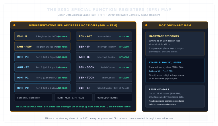
The 8051 Special Function Registers (SFR) Map
In the classic 8051, 21 distinct SFRs are distributed across this 128-address territory. Here are representative examples and their assigned memory addresses:
Address SFR Name Functional Role
80H P0 Port 0 Latch
81H SP Stack Pointer (initialized to 07H on Reset)
82H DPL Data Pointer Low Byte
83H DPH Data Pointer High Byte
87H PCON Power Control
88H TCON Timer/Counter Control
89H TMOD Timer/Counter Mode Configuration
90H P1 Port 1 Latch
98H SCON Serial Port Control
99H SBUF Serial Data Buffer (Tx / Rx)
A0H P2 Port 2 Latch
A8H IE Interrupt Enable Control
B0H P3 Port 3 Latch
B8H IP Interrupt Priority Control
D0H PSW Program Status Word (Flags & Bank Select)
E0H ACC Accumulator
F0H B B Register (Arithmetic Multiplication / Division)
Notice that these are examples, not a full list.
Each of these registers has a specific, fixed location in the memory map. When the processor writes to address E0H, it is writing to the Accumulator. When it writes to address 81H, it is updating the Stack Pointer. When it reads from address 99H, it is retrieving the latest byte received by the serial UART.
Furthermore, SFRs whose hexadecimal addresses end in 0H or 8H (such as 80H, 88H, 90H, 98H, A0H, A8H, B0H, B8H, D0H, E0H, F0H) are also bit-addressable.
This means an engineer can turn on an individual interrupt bit or read a single pin on Port 1 directly by its bit address, without altering any other bit in that register.
The essential point to establish here is simple:
These hardware control and status registers have addresses.
7. Not Everything Is RAM
This brings us to a crucial conceptual clarification.
Look at the two halves of the internal data-address space side by side:
Internal Data Address Space
00H–7FH → Internal RAM (Physical data memory)
80H–FFH → SFR Address Space (Hardware control and status)
Because both regions are addressed using numbers between 00H and FFH, it is easy to assume that they behave the same way.
They do not.
The fact that SFRs occupy addresses does not mean they are ordinary RAM.
Internal RAM (00H–7FH) consists of passive memory cells. When you write a byte into address 30H, the flip-flops store that value. When you read from 30H, you receive the exact same value back. Nothing else in the microcontroller changes.
When you access an SFR, you are communicating directly with physical hardware circuits.
Reading or writing an SFR causes the corresponding hardware block to respond.
Consider a simple instruction:
MOV P1, #0FFH
This instruction sends the hexadecimal value 0FFH to address 90H.
If address 90H were ordinary RAM, this would merely store eight 1s into eight memory cells.
Instead, address 90H is wired directly to the output latch of Port 1.
Writing 0FFH causes the Port 1 hardware to respond immediately. Internal transistors switch state, and high voltage levels (+5V) appear across eight physical metal pins protruding from the plastic package of the chip.
A single memory write has produced physical electrical action in the outside world.
Similarly:
- Writing to TCON (88H) starts or stops an on-chip hardware timer.
- Writing to SBUF (99H) loads a byte into a shift register that begins clocking serial bits out onto a wire.
- Writing to IE (A8H) arms or disarms the CPU's interrupt circuitry.
In addition, because only 21 SFRs are implemented in the classic 8051, large portions of the 80H–FFH space are empty. Reading from an unassigned address in this range does not return a stored variable; it returns indeterminate electrical noise.
SFRs look like memory on the programmer's map.
In silicon, they are the steering wheel of the machine.
8. One Address Space, Many Roles
Now we can step back and bring the complete addressing model together.
The 8051 does not have a confusing jumble of conflicting memory areas. It has a beautifully structured hierarchy:
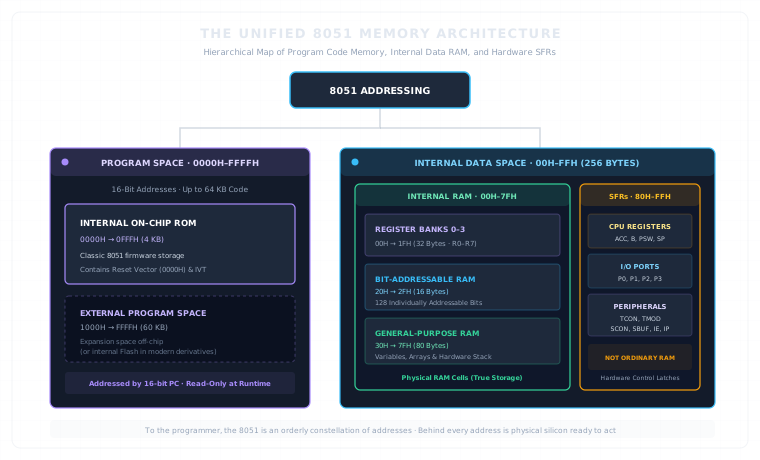
The Unified 8051 Memory Architecture
8051 ADDRESSING
│
┌────────────┴────────────┐
│ │
PROGRAM SPACE DATA SPACE
0000H–FFFFH Internal Data Space
│
┌──────────┴──────────┐
│ │
Internal RAM SFR Space
00H–7FH 80H–FFH
│
┌──────────┼──────────┐
│ │ │
Reg Banks Bit RAM General RAM
00–1F 20–2F 30–7F
Every piece has its place and its purpose:
1. Program Space (0000H–FFFFH): Addressed by the 16-bit Program Counter. In the classic 8051, the first 4 KB (0000H–0FFFH) lives on-chip, holding firmware instructions and vector tables. The remaining 60 KB is architectural expansion space.
2. Internal Data Space (00H–FFH): Addressed by 8-bit instructions, dividing the lower 128 bytes from the upper 128 addresses:
- Internal RAM (00H–7FH): Real storage cells for program execution:
- 00H–1FH: Four Register Banks of 8 working registers each (R0–R7).
- 20H–2FH: 16 bytes containing 128 individually addressable bit flip-flops.
- 30H–7FH: 80 bytes of general-purpose scratchpad memory and the system stack.
- SFR Space (80H–FFH): Memory-mapped control and status registers connecting the software directly to the CPU registers and peripheral hardware.
The entire chip is organized around this clean, predictable map.
9. The Programmer's View
To an electrical engineer inspecting silicon under a microscope, the 8051 is a microscopic city of transistors, diffusion layers, and metal interconnects.
To the programmer, the 8051 doesn't look like a collection of wires and transistors.
It looks like addresses.
An address can refer to program code.
It can refer to a byte in RAM.
It can refer to a register bank.
Or it can refer to a hardware control register.
Behind every address is hardware waiting to respond.
When the CPU reads address 0100H, program memory outputs an instruction opcode.
When the CPU writes to address 35H, internal RAM latches a variable.
When the CPU references R2, the active register bank supplies working data.
When the CPU writes to address 90H, physical pins turn on.
The memory map is the bridge between software logic and physical reality.
We've now found where the 8051 keeps its code, its data, and its control registers.
But the map raises another question.
What exactly are all these registers doing?
Current Exploration
The 8051 Memory Map