Controller
The 8051 — When Hardware Decides to Interrupt
How the classic 8051 turns physical events into priority-vectored CPU diversions.
Controller8051MicrocontrollerInterruptsTCONIEIPVectorsRETIEmbedded Systems
1. The Bits We Left Behind
In our exploration of 8051 timers, we examined the TCON register (88H).
We watched its upper four bits control time itself:
TCON (88H) — Upper Nibble (Timers)
├── Bit 7 (TF1) → Timer 1 Overflow Flag
├── Bit 6 (TR1) → Timer 1 Run Control
├── Bit 5 (TF0) → Timer 0 Overflow Flag
└── Bit 4 (TR0) → Timer 0 Run Control
Software toggled TR0 to start counting machine cycles, and hardware asserted TF0 when sixteen bits of silicon rolled over from FFFFH to 0000H.
Yet in that exploration, we deliberately left the lower four bits untouched:
TCON (88H) — Lower Nibble (Interrupts)
├── Bit 3 (IE1) → External Interrupt 1 Edge Flag
├── Bit 2 (IT1) → External Interrupt 1 Type Select
├── Bit 1 (IE0) → External Interrupt 0 Edge Flag
└── Bit 0 (IT0) → External Interrupt 0 Type Select
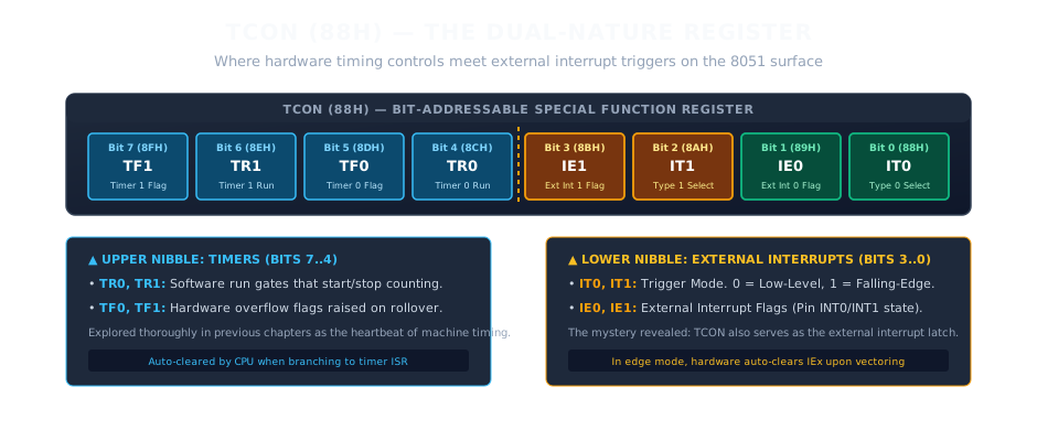
TCON Register Interrupt Controls
At first glance, this register seems strangely divided. Why did Intel's architects place external interrupt controls inside a register named Timer Control?
Because to digital silicon, a counter overflow and an external electrical pulse are cousin phenomena. Both are asynchronous physical transitions. Both signal that an event has occurred in the machine's environment. And both demand the immediate attention of the central processing unit.
Look closely at the lower nibble:
The Type Select Bits (IT0 and IT1)
Bits 0 and 2 configure how the microcontroller interprets voltage changes on its physical input pins (INT0 on pin P3.2, and INT1 on pin P3.3):
* When ITx = 0 (Low-Level Triggered): The 8051 samples the pin on every machine cycle. If the pin is held at a digital LOW level (0V), the hardware registers an active interrupt request. The signal must remain LOW until sampled, but it must return HIGH before the service routine completes, or the interrupt will immediately fire again.
* When ITx = 1 (Falling-Edge Triggered): Internal logic compares samples across consecutive machine cycles. When it detects a high-to-low transition (1 → 0), it automatically latches the event into silicon. A brief negative voltage spike is captured and held, even if the pin immediately returns HIGH.
The Edge Flags (IE0 and IE1)
Bits 1 and 3 act as hardware memories. When ITx = 1 and a falling edge arrives on an external pin, hardware automatically sets IEx = 1.
This bit remains high, holding the interrupt request steady while the CPU completes its current instruction. When the CPU finally accepts the request and branches to the corresponding vector address, the 8051's internal circuitry automatically clears IEx back to 0.
The switches were waiting on the surface of TCON all along. Now we explore the machinery they awaken.
2. The Five Voices
In our main-tree exploration When Hardware Learned to Interrupt, we uncovered the universal architectural shift that liberated computing: rather than forcing the CPU to burn millions of cycles repeatedly asking peripherals if they were ready, hardware was given a voice. Peripherals learned to raise an electrical signal, freeze the processor mid-stride, and demand service.
How did the classic Intel 8051 implement this principle in silicon?
The original 8051 architecture provides exactly five distinct interrupt sources:
THE FIVE VOICES OF THE 8051:
1. INT0 (External Pin P3.2)
2. Timer 0 (Internal Overflow TF0)
3. INT1 (External Pin P3.3)
4. Timer 1 (Internal Overflow TF1)
5. Serial (UART Receive RI / Transmit TI combined)
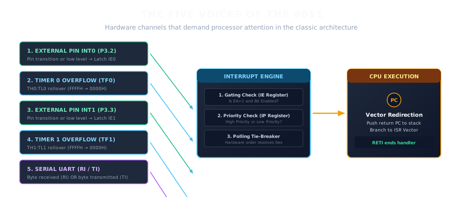
The Five Interrupt Sources of the 8051
Notice the symmetry in Intel's design:
* Two external physical pins (INT0, INT1) allow the outside world—sensors, emergency stop switches, optical encoders—to command the CPU directly.
* Two internal counters (Timer 0, Timer 1) allow the passage of time itself to divert program flow at precise, deterministic intervals.
* One communication channel (Serial Port) alerts the processor whenever a character has arrived over the serial line or when a transmitted character has cleared the shift register.
Five separate hardware blocks can raise a hand.
Yet the 8051 contains only one arithmetic logic unit and one Program Counter. It can execute only one instruction stream at a time. If all five voices shouted simultaneously without rules, the microcontroller would collapse into chaos.
Silicon requires an arbiter.
3. Who Is Allowed to Speak?
In an embedded system, hardware events occur continuously. Pins fluctuate with electrical noise, timers overflow repeatedly, and serial lines idle. If every voltage ripple immediately derailed the processor, no baseline software could ever finish executing.
There must be an administrative gateway that decides which voices are permitted to reach the CPU.
In the 8051, that gatekeeper is the IE (Interrupt Enable, A8H) register.
IE (A8H) — Bit-Addressable Interrupt Enable Register
┌──────┬──────┬──────┬──────┬──────┬──────┬──────┬──────┐
│ EA │ — │ — │ ES │ ET1 │ EX1 │ ET0 │ EX0 │
└──────┴──────┴──────┴──────┴──────┴──────┴──────┴──────┘
Bit 7 Bit 6 Bit 5 Bit 4 Bit 3 Bit 2 Bit 1 Bit 0
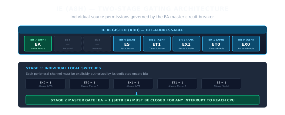
The IE Register Two-Stage Gating Mechanism
The 8051 implements a two-stage gating architecture:
Stage 1: Individual Channel Enables
Each interrupt source has its own dedicated on/off switch:
* EX0 (Bit 0): Enable External Interrupt 0
* ET0 (Bit 1): Enable Timer 0 Interrupt
* EX1 (Bit 2): Enable External Interrupt 1
* ET1 (Bit 3): Enable Timer 1 Interrupt
* ES (Bit 4): Enable Serial Port Interrupt
Setting a bit to 1 enables that individual source; clearing it to 0 silences it completely.
Stage 2: The Master Switch (EA)
At Bit 7 sits EA (Enable All).
In silicon, the signal line from each peripheral passes through an AND gate connected directly to EA. If EA = 0, the output of all five AND gates is held low. Not a single interrupt can reach the CPU, regardless of how EX0 or ET1 are configured.
Only when EA = 1 is the master circuit breaker closed, allowing individual enabled interrupts to pass through.
Why did hardware architects separate this into two stages?
Consider an embedded control loop updating motor calibration constants. If an interrupt fires halfway through the calculation, reading half-updated variables could destroy the mechanical actuator.
By having a single master switch EA, software can disable all interrupts with one single-cycle instruction (CLR EA), perform its atomic critical calculation, and re-enable them just as quickly (SETB EA)—without ever losing track of which individual peripherals were enabled.
4. When the Event Becomes a Request
An event is a physical occurrence in silicon: a voltage pulse transitions from 5V to 0V on pin P3.2, or an eight-bit register rolls over from FFH to 00H.
A request is a persistent bit waiting for CPU attention.
How does an event cross this boundary?
PHYSICAL EVENT LATCHED FLAG INTERRUPT VECTOR
Falling edge on P3.2 ────> IE0 in TCON (88H) ────> 0003H (INT0)
Timer 0 rolls over ────> TF0 in TCON (88H) ────> 000BH (Timer 0)
Falling edge on P3.3 ────> IE1 in TCON (88H) ────> 0013H (INT1)
Timer 1 rolls over ────> TF1 in TCON (88H) ────> 001BH (Timer 1)
Byte received/sent ────> RI / TI in SCON ────> 0023H (Serial)
Here lies one of the most critical subtleties of the 8051 architecture: the asymmetry of flag clearing.
Automatic Hardware Clearing
For Timer 0, Timer 1, and edge-triggered external interrupts (INT0 and INT1), Intel built automatic flag-clearing into the silicon.
When the CPU finishes its current instruction and vectors to 000BH to service Timer 0, internal hardware logic clears TF0 automatically. Software does not need to write CLR TF0. The very act of branching to the vector consumes and extinguishes the request.
Manual Software Clearing (The Serial Exception)
The serial interface behaves entirely differently.
Both byte reception (RI) and transmission completion (TI) share a single interrupt vector at 0023H. When the CPU vectors to 0023H, the silicon does not know which event triggered the jump. Did a new packet arrive from a sensor, or did the transmitter finish sending the previous byte?
Because hardware cannot deduce the cause, the 8051 never clears RI or TI automatically.
The programmer's service routine must inspect both flags, decide what action to take, and manually clear the flag using software instructions (CLR RI or CLR TI). If software fails to clear the flag, the moment the service routine exits, the CPU will immediately re-enter the exact same ISR in an infinite, locked loop.
5. When Two Voices Speak Together
What happens if an external sensor triggers INT0 at the exact same clock edge that Timer 0 overflows?
Both flags (IE0 and TF0) flip to 1 simultaneously. Both channels are enabled in IE. EA = 1.
The single Program Counter cannot jump to address 0003H and address 000BH at the same time. The hardware must make an unambiguous choice: which voice speaks first, and can one voice interrupt another?
To give developers control over this decision, the 8051 provides the IP (Interrupt Priority, B8H) register.
IP (B8H) — Bit-Addressable Interrupt Priority Register
┌──────┬──────┬──────┬──────┬──────┬──────┬──────┬──────┐
│ — │ — │ — │ PS │ PT1 │ PX1 │ PT0 │ PX0 │
└──────┴──────┴──────┴──────┴──────┴──────┴──────┴──────┘
Bit 7 Bit 6 Bit 5 Bit 4 Bit 3 Bit 2 Bit 1 Bit 0
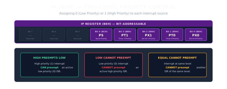
The IP Register and Priority Architecture
Every interrupt source has a corresponding bit in IP:
* PX0: Priority for External Interrupt 0
* PT0: Priority for Timer 0
* PX1: Priority for External Interrupt 1
* PT1: Priority for Timer 1
* PS : Priority for Serial Port
In the classic 8051, priority is strictly binary:
* 0 = Low Priority (the default state after hardware reset)
* 1 = High Priority
With this single register, software can partition the machine's five interrupt sources into two distinct operational classes.
6. The 8051’s Two Levels of Priority
What does assigning an interrupt to "High" or "Low" priority actually change inside the chip?
Many embedded developers assume priority only determines who gets serviced first during a tie. But in microcontroller design, priority has a far more profound meaning: preemption.
The 8051 silicon enforces three fundamental priority laws:
THE THREE LAWS OF 8051 INTERRUPT PRIORITY:
1. A High-Priority interrupt can PREEMPT (interrupt) an ongoing
Low-Priority interrupt service routine.
2. A Low-Priority interrupt can NEVER preempt an ongoing
High-Priority interrupt service routine.
3. An interrupt can NEVER preempt another interrupt of the
SAME priority level.
To enforce these laws, Intel's engineers did not write microcode loops. They placed two internal hardware status flip-flops directly into the processor core:
* Low-Priority Active Flip-Flop
* High-Priority Active Flip-Flop
These flip-flops are completely invisible to ordinary software instructions. When the CPU branches to a Low-priority vector, silicon automatically sets the Low-Priority Active flip-flop. While that flip-flop remains set, internal logic gates block all other Low-priority requests from reaching the CPU interrupt line. They are not forgotten; their flags remain latched in TCON, but they cannot divert the CPU.
Only an interrupt marked with a 1 in IP (High Priority) can bypass this gate and suspend the running routine.
7. When Everyone Has the Same Priority
When an 8051 powers up or undergoes a reset, every bit in the IP register is initialized to 00H. All five interrupt sources are set to Low Priority.
If Timer 0 and INT0 trigger at the exact same machine cycle under this condition, who wins?
When multiple pending requests share the same programmed priority level, the 8051 falls back to its built-in, hardwired Fixed Polling Sequence:
FIXED POLLING SEQUENCE (SAME-PRIORITY TIE-BREAKER):
1. INT0 (Highest Priority Tie-Breaker)
2. Timer 0
3. INT1
4. Timer 1
5. Serial (Lowest Priority Tie-Breaker)
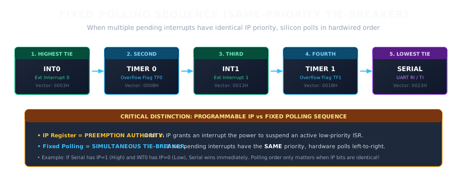
Fixed Polling Sequence vs Programmable IP
This polling chain is burned permanently into the silicon multiplexers of the chip.
The Crucial Distinction: IP vs Fixed Polling
One of the most frequent misconceptions in embedded architecture is confusing the fixed polling sequence with preemption authority:
* The IP Register grants PREEMPTION AUTHORITY. A High-priority interrupt has the physical power to suspend an active Low-priority service routine mid-execution.
* The Fixed Polling Sequence is strictly a TIE-BREAKER. It determines execution order only when simultaneous requests arrive with identical priority. It grants zero preemption authority!
Consider this concrete scenario:
Timer 0 (Low priority) is currently executing its service routine. While it is running, an external event asserts INT0 (also Low priority).
Even though INT0 sits higher than Timer 0 in the fixed polling sequence, INT0 cannot interrupt Timer 0. Because both share Low priority, the active status flip-flop holds INT0 at bay. INT0 must wait patiently until Timer 0 finishes completely.
Polling order only decides who gets picked when two requests are waiting at the door. IP decides who can kick the door down while someone else is inside.
8. Can an Interrupt Interrupt an Interrupt?
To see the priority architecture in its full elegance, watch what happens when an interrupt interrupts an ongoing interrupt.
Imagine an industrial controller:
* Timer 0 runs at Low Priority (PT0 = 0), updating an LED display every 5 milliseconds.
* INT1 is connected to an emergency thermal limit sensor and configured as High Priority (PX1 = 1).
Here is the chronological journey through silicon:
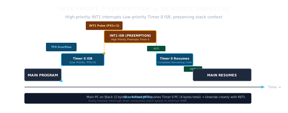
8051 Priority Nesting Timeline
1. MAIN PROGRAM EXECUTION
The CPU is executing the baseline application loop.
Program Counter (PC) advances instruction by instruction.
2. TIMER 0 OVERFLOWS (Low Priority)
- Hardware sets TF0 in TCON.
- CPU finishes its current instruction.
- Hardware pushes the 16-bit Main PC (2 bytes) onto the internal stack.
- Low-Priority Active flip-flop asserts.
- Hardware clears TF0 and vectors PC to 000BH.
- Timer 0 ISR begins running.
3. EMERGENCY PULSE ARRIVES ON INT1 (High Priority)
- Thermal sensor pulls INT1 low; hardware latches IE1.
- Silicon inspects IP: PX1 = 1 (High Priority).
- High Priority beats active Low Priority! Preemption granted.
- CPU freezes Timer 0 ISR immediately after its current instruction.
- Hardware pushes the current Timer 0 PC (2 bytes) onto the stack.
- High-Priority Active flip-flop asserts.
- Hardware clears IE1 and vectors PC to 0013H.
- Emergency INT1 ISR begins running.
4. INT1 ISR COMPLETES (RETI)
- INT1 routine finishes its emergency shutdown sequence.
- CPU executes RETI (Return from Interrupt).
- High-Priority Active flip-flop clears.
- Hardware pops 2 bytes from the stack back into PC.
- CPU seamlessly resumes the Timer 0 ISR exactly where it was frozen!
5. TIMER 0 ISR COMPLETES (RETI)
- Timer 0 routine finishes updating the display.
- CPU executes RETI.
- Low-Priority Active flip-flop clears.
- Hardware pops 2 bytes from the stack back into PC.
- CPU resumes the Main Program.
The Cost in Internal RAM
Notice what happened to the stack during nesting:
* The main program return address consumed 2 bytes of stack.
* The nested Timer 0 return address consumed another 2 bytes of stack.
In the classic 8051, the entire internal data RAM is only 128 bytes, shared between register banks, bit-addressable variables, user scratchpad memory, and the hardware stack (SP).
If an interrupt service routine also saves registers (PUSH ACC, PUSH PSW, PUSH DPH), each nested level eats deeper into internal memory. Without careful stack budgeting, nested interrupts can silently overwrite application variables—one of the most elusive bugs in early embedded engineering.
9. Where Does the CPU Go?
When the 8051 accepts an interrupt request, where does it send the Program Counter?
In modern complex operating systems, interrupt vectors are often stored as a table of 32-bit pointers in RAM. But on the 8051, there was no RAM to spare.
Instead, Intel's architects etched the vector entry points directly into the lowest addresses of Program ROM:
8051 INTERRUPT VECTOR TABLE:
ROM ADDRESS INTERRUPT SOURCE
─────────── ───────────────────────────────
0000H System Reset (Power-On / RST Pin)
0003H External Interrupt 0 (INT0)
000BH Timer 0 Overflow (TF0)
0013H External Interrupt 1 (INT1)
001BH Timer 1 Overflow (TF1)
0023H Serial Port (RI + TI)
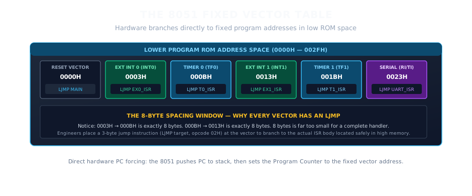
8051 Interrupt Vector Table
Look closely at the addresses. Calculate the distance between them:
000BH - 0003H = 8 Bytes
0013H - 000BH = 8 Bytes
001BH - 0013H = 8 Bytes
0023H - 001BH = 8 Bytes
Each vector slot is separated by exactly 8 bytes of memory.
The 8-Byte Problem
Why 8 bytes? Intel's engineers wanted to give developers enough room to write a tiny, self-contained handler—such as toggling an output pin and returning—directly at the vector address without branching elsewhere.
In real-world systems, however, 8 bytes is rarely enough. A typical ISR must save the accumulator, inspect flags, update a counter, restore registers, and execute RETI—easily taking 20 to 50 bytes of code. If your code exceeds 8 bytes, it physically spills into the memory reserved for the next interrupt vector!
To solve this, the universal convention in 8051 software is to place a single 3-byte Long Jump instruction (LJMP) at each vector:
ORG 0000H
LJMP MAIN ; 3 bytes: Jump over vector table to main code
ORG 0003H
LJMP EXT0_ISR ; 3 bytes: Jump to actual External 0 handler
ORG 000BH
LJMP TIMER0_ISR ; 3 bytes: Jump to actual Timer 0 handler
An LJMP instruction requires exactly 3 bytes (1 byte opcode + 2 bytes destination address). It fits comfortably within the 8-byte window, cleanly vaulting the execution stream out of the vector table and into open code memory where the full service routine can live.
10. From Vector to ISR
In microprocessor assembly programming, subroutines end with the return instruction: RET.
Yet every 8051 interrupt service routine must end with a different instruction: RETI (Return from Interrupt).
Why did Intel create two separate return instructions?
RET:
├── Pops 2 bytes from Stack → Program Counter (PC)
└── Execution resumes at caller address
RETI:
├── Pops 2 bytes from Stack → Program Counter (PC)
├── Execution resumes at caller address
└── CLEARS INTERNAL SILICON PRIORITY STATUS FLIP-FLOP!
Both instructions perform the exact same stack operation: they pop two bytes from the stack pointer and restore them into the Program Counter.
The difference lies entirely in the silicon arbiter:
When an interrupt begins, the 8051 hardware asserts an internal priority status flip-flop to block incoming interrupts of the same or lower rank.
RET knows nothing about interrupts. If a programmer mistakenly writes RET at the end of an ISR:
1. The CPU pops the Program Counter and successfully returns to the main program loop.
2. The main program continues executing as if nothing happened.
3. However, the internal priority flip-flop remains asserted in silicon!
Because that flip-flop is still set, the 8051 believes it is still executing an interrupt service routine. It will permanently block all future interrupts of that priority level and all lower priority levels. The timers may overflow and external pins may pulse, but the CPU will remain deaf to them forever until the chip is physically reset.
RETI is an essential architectural handshake. It does not merely restore the Program Counter; it informs the hardware arbiter:
"The service routine is finished. Clear the priority lock. Re-open the gate."
11. The Deeper Realization
When you look across the entire 8051 interrupt subsystem, you realize it is not a collection of isolated features. It is a carefully orchestrated dialogue between hardware physics and software policy:
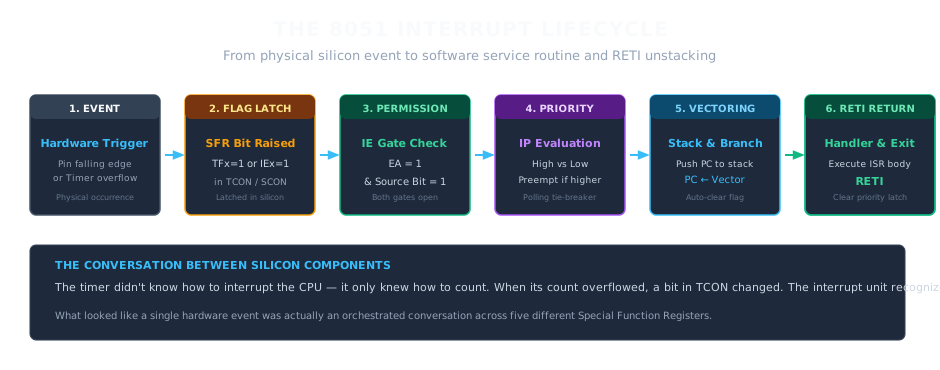
Complete 8051 Interrupt Lifecycle Flow
1. A physical transition occurs (pin falls low, counter overflows).
2. TCON or SCON latches the event into a request flag.
3. IE verifies both local and global permission switches.
4. IP arbitrates between competing requests and active priority locks.
5. The CPU completes its current instruction, saves PC, and vectors to low ROM.
6. The vector LJMP vaults program flow into the service routine.
7. Software performs its emergency response.
8. RETI unwinds the stack and releases the hardware priority arbiter.
In modern computing, we take multi-level nested interrupts, priority preemptions, and vector dispatching for granted. High-performance processors use hundreds of interrupt channels managed by dedicated nested vector interrupt controllers.
Yet inside the classic 40-pin 8051, Intel captured the fundamental grammar of machine interruptions:
* Two physical triggers (level vs edge)
* Two-stage gating (individual vs master)
* Two priority levels (cooperative polling vs preemptive nesting)
* Fixed-space vector tables
* And atomic hardware-software handshakes (RETI)
Software establishes the rules—configuring modes in TCON, permissions in IE, and rank in IP.
Once those rules are set, hardware executes them at the speed of silicon, ensuring that when the physical world speaks, the processor listens without missing a beat.
Current Exploration
The 8051 — When Hardware Decides to Interrupt