Controller
The 8051 — Where Software Touches Hardware
How Special Function Registers connect software to the CPU, peripherals, and physical world.
Controller8051MicrocontrollerSFRSpecial Function RegistersHardware InterfaceArchitectureEmbedded Systems
1. The Addresses Above 7FH
In our previous exploration, we walked through the 8051 memory map.
We saw how internal data memory is divided into two distinct regions at address 7FH:
DATA MEMORY (00H–FFH)
│
├── 00H–7FH → Internal RAM (Register Banks, Bit RAM, Scratchpad)
│
└── 80H–FFH → Special Function Register (SFR) Address Space
Below 80H, every location represents real, physical static RAM cells. Address 00H through 1FH holds four register banks of working registers (R0–R7). Address 20H through 2FH holds 128 bit-addressable storage cells. Address 30H through 7FH holds general scratchpad storage and the system stack.
If you write a byte to address 35H, it stays there quietly. If you read it back, you get the exact value you stored. It is passive memory.
But then we crossed address 7FH.
Above 7FH—from 80H to FFH—lies another 128 addresses.
And here, the nature of memory changes completely.
80H–FFH IS NOT ORDINARY RAM
We crossed 7FH. But what changed?
When the 8051 CPU places an address like 80H, 88H, 90H, or E0H onto its internal bus, it is not reaching into a passive data buffer. It is speaking directly to Special Function Registers (SFRs).
Special Function Registers are the software control surface of the microcontroller. They are the physical registers that connect the CPU core to its computational machinery, to on-chip peripherals, and to the external pins that touch the outside world:
P0 (80H) → Port 0 Parallel I/O
SP (81H) → Stack Pointer
DPL (82H) → Data Pointer Low Byte
DPH (83H) → Data Pointer High Byte
PCON (87H) → Power Control Register
TCON (88H) → Timer / Counter Control Register
TMOD (89H) → Timer / Counter Mode Register
P1 (90H) → Port 1 Parallel I/O Latch
SCON (98H) → Serial Port Control Register
SBUF (99H) → Serial Data Buffer (Tx / Rx)
IE (A8H) → Interrupt Enable Register
IP (B8H) → Interrupt Priority Register
PSW (D0H) → Program Status Word
ACC (E0H) → Accumulator Register
B (F0H) → B Register (Arithmetic Partner)
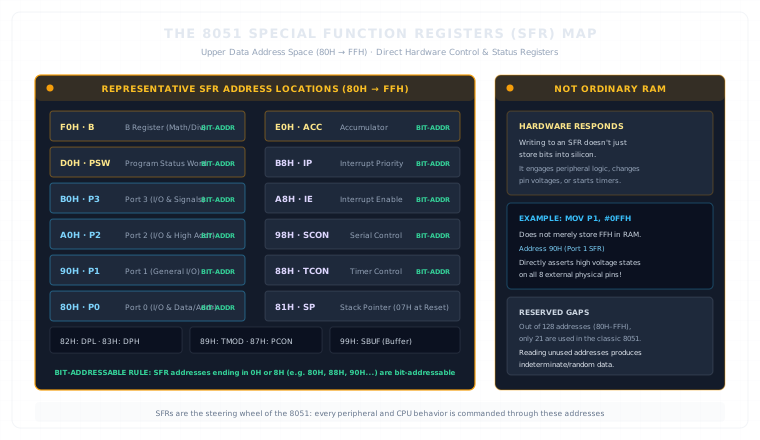
The 8051 Special Function Register Map
Every one of these registers is wired to active silicon hardware.
And that changes the meaning of what a register actually is.
2. A Register With a Job
What fundamentally makes an SFR different from ordinary RAM?
An ordinary RAM location is passive storage. It has no responsibilities. It holds whatever value software deposited into it until power is removed or a new byte overwrites it. Address 42H does not care whether you store an ASCII character, a mathematical variable, or an array offset; to the RAM, every byte is just bits of stored charge.
An SFR is active. An SFR has a job.
An SFR is an electrical gateway between software instructions and a specific hardware mechanism inside the chip:
WRITING TO AN SFR
• Writing to P1 → Controls physical I/O pins.
• Writing to TCON → Starts, stops, or configures the hardware timers.
• Writing to SCON → Sets UART communication framing and enables the receiver.
• Writing to IE → Arms or disarms CPU interrupt gates.
• Writing to PSW → Switches the active working register bank in internal RAM.
The relationship works in both directions.
When software reads ordinary RAM, it simply retrieves what was written earlier. But when software reads an SFR, it often observes dynamic, real-time hardware state:
READING FROM AN SFR
• Reading P1 → Observes electrical logic levels present on external pins.
• Reading TL0 → Observes elapsed clock pulses counted by hardware timers.
• Reading SCON → Discovers whether a serial character has arrived over wires.
• Reading PSW → Inspects ALU condition flags from recent calculations.
RAM is a storage cabinet. An SFR is an instrument panel with switches and live gauges.
3. The Machine's Control Surface
To the software developer, the upper address space of the 8051 appears as an organized control surface.
Rather than inventing proprietary hardware control instructions for every internal subsystem, Intel's architects mapped every peripheral and CPU core control mechanism into the upper data memory space: 80H–FFH.
Across this space, exactly 21 Special Function Registers are implemented in the classic 8051 architecture:
THE 8051 CONTROL SURFACE
│
┌───────────┬───────────┬───────┴───┬───────────┬───────────┬───────────┐
│ │ │ │ │ │ │
CPU I/O TIMERS SERIAL INTERRUPTS POWER POINTERS
Core Ports & Counters Port Control Control (16-bit)
│ │ │ │ │ │ │
ACC P0 TCON SCON IE PCON DPL
B P1 TMOD SBUF IP DPH
PSW P2 TL0 SP
P3 TH0
TL1
TH1
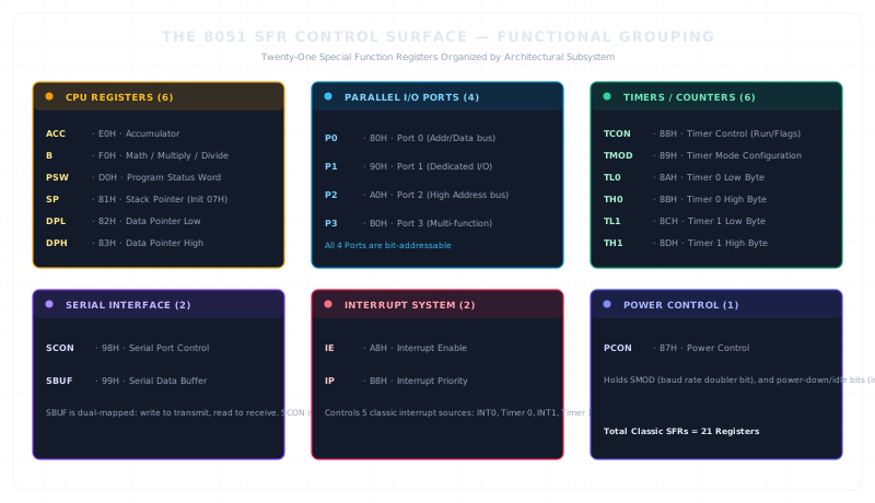
The 8051 Special Function Register Subsystems
The SFR map is effectively a map of the 8051's internal capabilities.
Notice how subsystems like Timers, the Serial Port, and the Interrupt Controller appear here as closed doorways. Their registers are present in the map, waiting for software to command them.
4. The CPU Has Addresses Too
The first group of SFRs does not interface with the outside world. They control the central processing unit itself:
ACC (E0H) → Accumulator
B (F0H) → B Register (Arithmetic Partner)
PSW (D0H) → Program Status Word
SP (81H) → Stack Pointer
DPL (82H) → Data Pointer Low Byte
DPH (83H) → Data Pointer High Byte
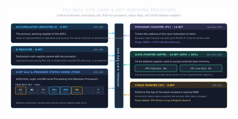
The 8051 CPU Core Registers
Each of these has a distinct architectural role:
- ACC (E0H) is the primary computational register. Almost every arithmetic and logical instruction in the 8051 uses the Accumulator as one of its operands and destination.
- B (F0H) serves as a general register, but has a dedicated hardwired relationship with ACC for hardware multiplication (MUL AB) and division (DIV AB).
- PSW (D0H) stores arithmetic condition flags like Carry (CY) and Overflow (OV). Crucially, bits RS1 and RS0 select which of the four register banks in internal RAM is currently active. By altering two bits in PSW, software reassigns the working register set R0–R7 without moving a single data byte.
- SP (81H) manages the system stack, which grows upward in internal RAM. On reset, SP initializes to 07H—the top of Register Bank 0—meaning the first push naturally targets address 08H.
- DPTR (DPH 83H + DPL 82H) combines two 8-bit registers into a 16-bit pointer. This gives an 8-bit core the architectural reach to access up to 64 KB of external data memory or code lookup tables.
Even the core mechanics of the processor are operated through addresses.
5. Four Doors to the Outside
The 8051 connects to external circuits through 32 physical pins arranged as four 8-bit parallel I/O ports:
P0 (80H) → Port 0 (Pins 32–39)
P1 (90H) → Port 1 (Pins 1–8)
P2 (A0H) → Port 2 (Pins 21–28)
P3 (B0H) → Port 3 (Pins 10–17)
Each port has a corresponding Special Function Register at its base address. Writing to the register updates the pins; reading from it inspects incoming external signals.
These four ports are not identical:
- Port 1 (90H) is a dedicated general-purpose parallel I/O port. In the classic 8051, pins P1.0 through P1.7 serve solely as digital input and output lines.
- Port 0 (80H) & Port 2 (A0H) serve as the external memory bus. When external memory is attached, Port 0 carries multiplexed low-order addresses and data, while Port 2 provides high-order addresses.
- Port 3 (B0H) is multifunctional. Beyond general I/O, its pins carry vital peripheral lines: serial communication (RXD, TXD), external interrupt triggers (INT0, INT1), timer clock inputs (T0, T1), and external memory read/write strobes (RD, WR).
The four ports are the doors through which internal software reaches external reality.
6. The Hardware Hiding Behind an Address
Consider the pattern that has begun to emerge:
90H → P1 → I/O Port Hardware
88H → TCON → Timer / Counter Hardware
98H → SCON → Serial Communication Hardware
A8H → IE → Interrupt Control Hardware
Behind each of these addresses sits an independent silicon subsystem.
When software writes to 88H (TCON), it is not storing numbers. It is turning timer clock gates on or off.
When software writes to 98H (SCON), it is configuring the framing rate and receiver circuits of the on-chip UART.
When software writes to A8H (IE), it is arming or disarming the CPU's interrupt sensitivity.
The unifying principle remains the same across every peripheral:
Software → Address → SFR → Hardware Subsystem
The CPU does not require custom wiring or specialized machine instructions for each new device. An address is all that is needed.
7. Where Bits Become Control
In desktop computing, memory is accessed in 32-bit or 64-bit words. Modifying a single control flag requires loading the word, applying a bitmask, and writing it back.
In embedded systems, however, machines are controlled bit by bit:
- Turn on a motor relay.
- Start a hardware timer.
- Check if a serial character has arrived.
- Enable an external interrupt.
To make physical control fast and efficient, the 8051 makes certain SFRs bit-addressable.
How do you know which SFRs are bit-addressable?
The 8051 architecture follows a clean rule:
THE BIT-ADDRESSABLE SFR RULE:
An SFR is bit-addressable if and only if its
hexadecimal address ends in 0H or 8H.
Mathematically, any SFR address where Address MOD 8 == 0 can be addressed bit by bit.
Exactly 11 SFRs satisfy this rule in the classic 8051:
80H (P0), 88H (TCON), 90H (P1), 98H (SCON), A0H (P2), A8H (IE), B0H (P3), B8H (IP), D0H (PSW), E0H (ACC), and F0H (B).
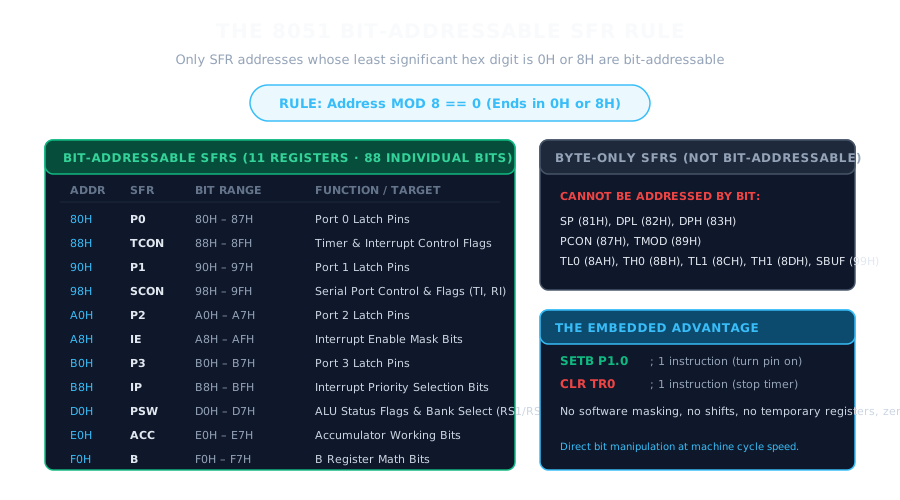
The 8051 Bit-Addressable SFR Rule
All other SFRs—such as SP (81H), TMOD (89H), and SBUF (99H)—are byte-only.
This architectural feature allows single-instruction atomic operations:
SETB P1.0 ; Turn on Pin 1.0 directly
CLR TR0 ; Stop Timer 0 directly
A single instruction manipulates a single hardware bit in a single cycle, with no temporary registers and no risk of disturbing neighboring bits.
This bit-level authority will become deeply relevant when we encounter timer run bits, interrupt masks, and communication status flags.
8. The Other Side of the Machine
The same architectural philosophy extends across every corner of the chip:
TIMERS: TCON, TMOD, TH0, TL0, TH1, TL1
SERIAL PORT: SCON, SBUF
INTERRUPTS: IE, IP
- Timers: Rather than forcing the CPU to burn cycles in empty delay loops, hardware counters (TL0/TH0 and TL1/TH1) increment automatically in silicon on every clock cycle. Software configures them via TMOD and commands them via TCON.
- Serial Port: Two independent hardware shift registers share the address SBUF (99H)—one for transmitting outgoing bytes, one for receiving incoming bytes—supervised by control register SCON.
- Interrupts: When time-critical events occur, hardware triggers the CPU directly. Software governs which events are allowed to interrupt via IE, and sets their priority order via IP.
Different hardware. Different assignments.
Yet every subsystem obeys the exact same pattern: software reaches hardware through an address.
9. Not Every Address Is a Register
Step back and consider the arithmetic of the upper data space:
SFR Address Space: 80H to FFH → 128 Addresses
Implemented SFRs: → 21 Registers
Unimplemented Addresses: → 107 Addresses
Out of 128 available addresses above 7FH, only 21 are wired to real registers in the classic 8051.
What lives at the other 107 addresses?
Nothing.
They are unimplemented address space.
ADDRESS SPACE ≠ IMPLEMENTED REGISTERS
An address space represents the numerical range that the internal address bus can express. It does not mean physical transistors exist at every location.
In the classic 8051:
- Writing to an unimplemented SFR address discards the byte. No silicon latch exists to catch it.
- Reading from an unimplemented address returns indeterminate, floating bus data.
Unimplemented SFR addresses must never be treated as scratchpad RAM. They are reserved voids in the silicon map—space where later derivative chips placed additional timers, analog-to-digital converters, and watchdog registers.
10. When an Address Becomes Hardware
We have arrived at the conceptual core of Special Function Registers.
Look once more at the addresses we have explored:
Address 30H → Scratchpad RAM → Stores passive data
Address 90H → Port 1 SFR → Controls physical pin voltages
Address 88H → TCON SFR → Gates clock pulses into a hardware counter
Address 98H → SCON SFR → Configures serial communication
Address A8H → IE SFR → Arms asynchronous interrupt triggers
The number itself—whether 30H, 88H, or 90H—has no innate magic.
An address is merely a numerical pattern of bits on an internal bus.
What gives that address meaning is the silicon architecture behind it.
Inside the microcontroller, an address decoder inspects the binary number generated by an instruction:
- If the address falls between 00H and 7FH, the decoder routes the signal to static RAM flip-flops.
- If the address is 90H, the decoder pulses the clock line of Port 1's output latches.
- If the address is 88H, the decoder enables the control inputs of the timer prescalers.
The address decoder is a translator of reality: it turns abstract numerical instructions into physical silicon behavior.
In desktop computing, software is heavily insulated from hardware by operating systems, virtual memory managers, and driver abstraction layers.
In an 8051 microcontroller, that insulation disappears.
When you write to an address, you are asserting direct electrical control over physical transistors.
11. Where Software Touches the Machine
The memory map showed us where the pieces of the 8051 live.
The Special Function Registers reveal something more interesting.
To the programmer, they look like ordinary addresses.
Inside the machine, they are connections to things that are actively doing work.
A byte written to RAM can simply remain a byte.
A byte written to an SFR can start a timer, change a physical pin, alter a processor state, or instruct a peripheral how to behave.
The address is only the beginning.
What lies behind it is the machine.
Current Exploration
The 8051 — Where Software Touches Hardware