Controller
The 8051 — When the Controller Learns to Speak
How the classic 8051 turns timers, dual buffers, and nine-bit frames into a complete serial subsystem.
Controller8051MicrocontrollerSerialUARTUSARTSCONSBUFTimer 1Baud RateEmbedded Systems
1. The 8051 Learns to Speak
In our main-tree exploration UART: Structured Asynchronous Communication, we discovered how two isolated electronic systems can converse over a single wire. By agreeing on a shared temporal rhythm, framing data with a leading start bit, and sealing it with a trailing stop bit, raw electrical voltages transformed into structured, intelligible data.
Later, in The Roads Not Often Travelled, we saw that communication does not have to remain purely asynchronous. A Universal Synchronous/Asynchronous Receiver/Transmitter (USART) can also transmit a dedicated clock signal alongside data, stripping away start and stop overhead to stream bytes at blistering bus speeds.
Now we return to the classic Intel 8051.
Having explored its memory map, special function registers, internal timers, and interrupt subsystem, we arrive at the periphery of the chip. How did Intel's architects implement serial communication in silicon?
The 8051 contains a full, hardware-implemented serial port wired to two physical pins on Port 3:
* Pin P3.1 (TXD): Transmit Serial Data
* Pin P3.0 (RXD): Receive Serial Data
Yet the 8051's serial port is not just an ordinary asynchronous UART.
Just as the 8051's internal timer could reshape its silicon into four distinct counting topologies, its serial port can operate across four distinct serial personalities:
THE SERIAL SPECTRUM OF THE 8051:
├── Mode 0 → Synchronous Shift Register (Half-Duplex I/O Expansion)
├── Mode 1 → Standard 8-Bit Asynchronous UART (Variable Baud Rate)
├── Mode 2 → 9-Bit Asynchronous UART (Fixed Baud Rate)
└── Mode 3 → 9-Bit Asynchronous UART (Variable Baud Rate)
The 8051 does not always have to behave like the asynchronous UART we already explored. In Mode 0, it behaves like the synchronous side of a USART—outputting its own clock to shift data into external chips. In Modes 1, 2, and 3, it speaks the familiar language of framed asynchronous pulses.
To control this chameleon hardware, the microcontroller exposes two dedicated Special Function Registers: SCON and SBUF.
2. The Registers Behind the Conversation
Continuing our journey across the 8051's Special Function Register surface, we meet SCON (Serial Control, 98H).
Like TCON and IE, SCON is completely bit-addressable. Every bit represents a direct silicon switch or a live status flag:
SCON (98H) — Bit-Addressable Serial Control Register
┌──────┬──────┬──────┬──────┬──────┬──────┬──────┬──────┐
│ SM0 │ SM1 │ SM2 │ REN │ TB8 │ RB8 │ TI │ RI │
└──────┴──────┴──────┴──────┴──────┴──────┴──────┴──────┘
Bit 7 Bit 6 Bit 5 Bit 4 Bit 3 Bit 2 Bit 1 Bit 0
(9FH) (9EH) (9DH) (9CH) (9BH) (9AH) (99H) (98H)
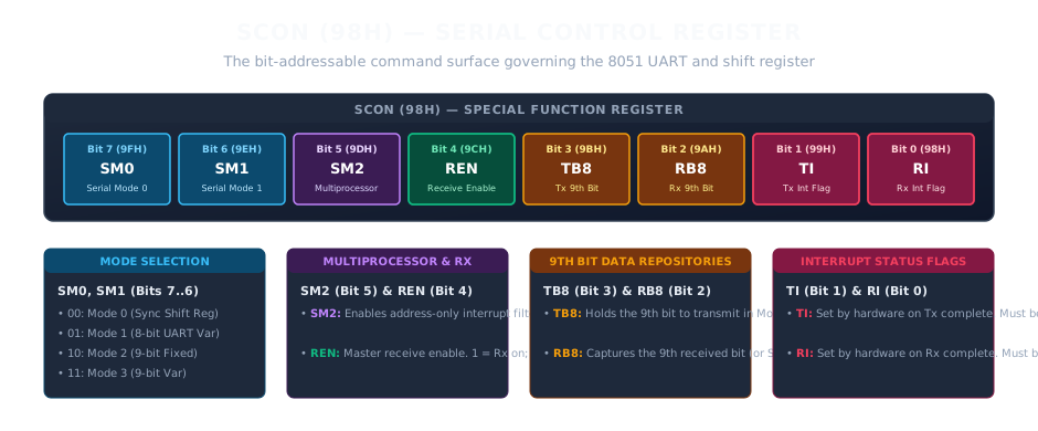
SCON Register Controls
Rather than treating SCON as a dry reference table, look at how its bits divide naturally into four functional teams:
1. Mode Selectors (SM0 and SM1)
Bits 7 and 6 dictate the fundamental operating mode of the serial hardware:
* SM0 = 0, SM1 = 0 → Mode 0: Synchronous 8-bit shift register.
* SM0 = 0, SM1 = 1 → Mode 1: 8-bit UART with variable baud rate.
* SM0 = 1, SM1 = 0 → Mode 2: 9-bit UART with fixed baud rate.
* SM0 = 1, SM1 = 1 → Mode 3: 9-bit UART with variable baud rate.
2. Multiprocessor & Reception Controls (SM2 and REN)
* SM2 (Bit 5): Enables the 8051's multiprocessor communication feature in Modes 2 and 3. When set, it instructs the receiver hardware to ignore incoming bytes unless their 9th bit is asserted.
* REN (Bit 4): Receiver Enable. Software holds the master key to the receive pin. Setting REN = 1 enables the 8051 to sample incoming bits on RXD. If software clears REN = 0, the receiver hardware disconnects internally, ignoring all incoming bus traffic.
3. The Ninth-Bit Transporters (TB8 and RB8)
* TB8 (Bit 3): Transmit Bit 8. In 9-bit modes (Modes 2 and 3), software writes the 9th data bit directly into this flip-flop before transmission.
* RB8 (Bit 2): Receive Bit 8. In Modes 2 and 3, hardware latches the 9th incoming data bit here. In Mode 1, if SM2 = 0, RB8 stores the received stop bit.
4. The Interrupt Status Flags (TI and RI)
* TI (Bit 1): Transmit Interrupt Flag. Hardware automatically asserts TI = 1 when it has finished transmitting a character.
* RI (Bit 0): Receive Interrupt Flag. Hardware automatically asserts RI = 1 when an incoming character has been completely received and assembled.
These eight bits form the command bridge of the serial port. But where does the actual data live?
3. One Register Name, Two Directions
When software wants to send or receive a character, it addresses SBUF (Serial Data Buffer, 99H).
Here we uncover one of the most elegant architectural illusions in the 8051:
Software writes to SBUF (MOV SBUF, A) ────> Transmit Shift Register
Software reads from SBUF (MOV A, SBUF) <──── Receive Buffer Latch
To the assembly programmer, SBUF appears to be a single eight-bit RAM register at address 99H.
In silicon, however, there is no single register named SBUF.
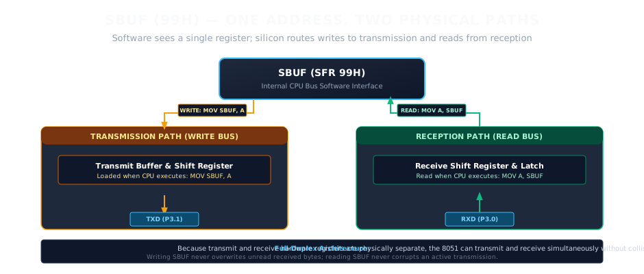
SBUF Dual Architecture
Intel's engineers mapped two completely separate physical registers to the same byte address:
* A write-only Transmit Buffer, wired to the parallel-load inputs of the transmit shift register.
* A read-only Receive Buffer, wired to the output latches of the receive shift register.
When the CPU executes:
MOV SBUF, A ; Write bus asserts: data flows into Transmit Register
the internal bus directs the accumulator's bits into the transmit shift register, automatically initiating serial transmission onto TXD (P3.1).
When the CPU executes:
MOV A, SBUF ; Read bus asserts: data flows from Receive Latch
the internal bus reads the contents of the receive buffer holding the most recently completed incoming byte from RXD (P3.0).
Why Separate the Paths?
This physical separation provides true Full-Duplex capability.
The 8051 can be actively serializing and shifting an outgoing byte out of TXD while simultaneously receiving and assembling an incoming byte from RXD. Because the transmit and receive buffers are physically distinct:
* Writing to SBUF never overwrites an unread received character waiting in the receive buffer.
* Reading SBUF never interrupts or corrupts an active transmission in progress.
One address on the software map opens two independent pipelines into the physical world.
4. Four Modes, Four Personalities
By writing different combinations to SM0 and SM1 in SCON, software reconfigures the internal data paths and timing sources of the serial hardware:
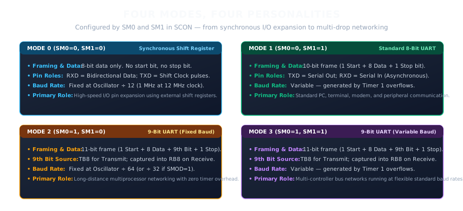
Four Serial Modes of the 8051
Mode 0 — Synchronous Shift Register (SM0 = 0, SM1 = 0)
In Mode 0, the 8051 abandons asynchronous framing entirely.
It operates as an 8-bit synchronous shift register:
* Data is transmitted and received solely through RXD (P3.0) as a bidirectional data line.
* TXD (P3.1) outputs a continuous shift clock.
* Exactly 8 bits are shifted in or out, Least Significant Bit (LSB) first.
* There are no start bits, no parity bits, and no stop bits.
* The baud rate is completely fixed: exactly one-twelfth of the oscillator frequency (f_osc ÷ 12). On a classic 12 MHz 8051, Mode 0 shifts data at a rapid 1 Mbit/s!
Why Synchronous Shift Register Mode?
Why would a microcontroller include a serial mode that cannot talk to a PC's serial port?
Mode 0 was designed for low-cost hardware pin expansion.
By connecting TXD (clock) and RXD (data) to an external serial-in, parallel-out shift register (such as the ubiquitous 74HC595), the 8051 can control eight, sixteen, or thirty-two external output pins—driving LED displays, relays, or motor drivers—using only two physical pins on the microcontroller!
Writing a byte to SBUF automatically clocks out eight pulses on TXD, filling the external shift register at wire speed without software ever toggling a GPIO pin manually.
Mode 1 — The UART We Recognize (SM0 = 0, SM1 = 1)
Mode 1 is the standard asynchronous serial communication format used to talk to computers, modems, GPS modules, and external microcontrollers.
In Mode 1:
* Communication is asynchronous and full-duplex (TXD sends, RXD receives).
* Each character is packaged in a 10-bit frame:
* 1 Start Bit (logic LOW)
* 8 Data Bits (LSB first)
* 1 Stop Bit (logic HIGH)
* The baud rate is variable—governed dynamically by the overflow rate of Timer 1.
As we explored in UART: Structured Asynchronous Communication, the receiver hardware on RXD does not simply sample the line once. It synchronizes on the falling edge of the start bit, oversamples the wire at 16 times the bit rate, and latches the data bits at their stable centers.
When the full byte arrives and the stop bit is detected, hardware transfers the 8 data bits into the receive buffer of SBUF, captures the stop bit into RB8, and asserts RI = 1.
Mode 2 — When One More Bit Appears (SM0 = 1, SM1 = 0)
Mode 2 expands the frame from 10 bits to 11 bits:
* 1 Start Bit (logic LOW)
* 8 Data Bits (LSB first)
* 1 Programmable 9th Bit
* 1 Stop Bit (logic HIGH)
Where does this extra ninth bit come from?
* On transmission, whatever bit software wrote into TB8 in SCON is automatically appended immediately after the 8th data bit.
* On reception, the received 9th bit is automatically captured into RB8 in SCON.
Mode 2 runs at a fixed baud rate:
* If SMOD = 0 in PCON, baud rate = f_osc ÷ 64.
* If SMOD = 1 in PCON, baud rate = f_osc ÷ 32.
Because its timing is derived directly from the master crystal oscillator through a fixed divider, Mode 2 operates completely independently of internal timers. Both Timer 0 and Timer 1 remain 100% free for application timing.
Mode 3 — The Other 9-Bit Voice (SM0 = 1, SM1 = 1)
Mode 3 is the architectural twin of Mode 2:
* It uses the exact same 11-bit frame (1 start bit, 8 data bits, programmable 9th bit via TB8/RB8, 1 stop bit).
* But instead of a fixed baud rate, its baud rate is variable, driven dynamically by Timer 1 overflows just like Mode 1.
Mode 3 combines the framing flexibility of the 9th bit with the custom speed tuning of an internal timer.
Why did Intel build two whole modes (Mode 2 and Mode 3) around an extra ninth bit?
5. The Ninth Bit Has a Secret
In single-device systems, an 8-bit frame is sufficient. You send eight bits of ASCII text or binary measurements, and the receiver consumes them.
The 9th bit exists because of a classic embedded engineering challenge: Multiprocessor Networking.
Imagine an automated factory floor where one master 8051 controller is wired over a shared two-wire RS-485 bus to ten slave 8051 microcontrollers controlling individual conveyor belts:
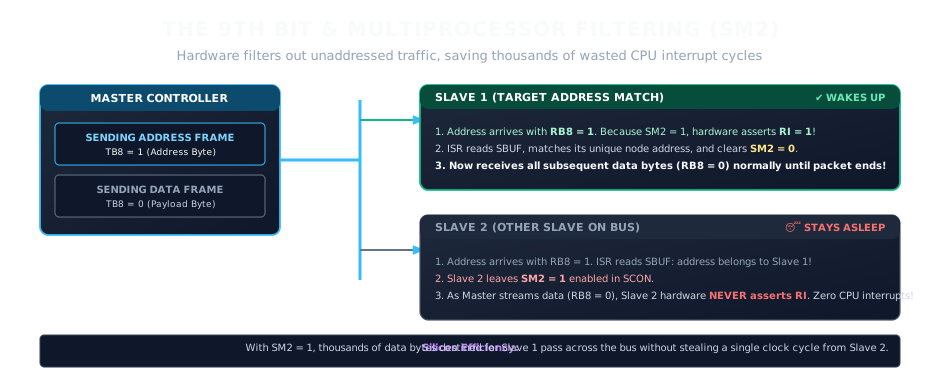
Multiprocessor SM2 Filtering Flow
Every slave controller has its RXD pin tied to the common bus.
If the master wants to send a 50-byte command packet to Slave 3:
* In a naive 8-bit protocol, every single byte sent across the bus would trigger a serial receive interrupt on all ten slaves.
* Slaves 1, 2, 4, 5... 10 would have their critical real-time motor control loops interrupted fifty times each—wasting thousands of instruction cycles reading bytes that don't belong to them!
Intel solved this elegantly in silicon using the 9th bit and the SM2 bit in SCON:
THE MULTIPROCESSOR CONVENTION:
├── 9th Bit = 1 (TB8 = 1) → The byte is an ADDRESS frame.
└── 9th Bit = 0 (TB8 = 0) → The byte is a DATA payload frame.
The Hardware Filter in Silicon
When slave controllers initialize, they set SM2 = 1 in their SCON registers.
When SM2 = 1 in Mode 2 or Mode 3, the 8051 receiver hardware activates an internal gate:
* The hardware asserts RI = 1 (triggering an interrupt) ONLY IF the received 9th bit (RB8) is 1.
* If a frame arrives with RB8 = 0, the silicon silently discards the frame! RI is never asserted, and the CPU is never interrupted.
Watch the protocol dance unfold:
1. The Master Calls an Address:
The master controller sets TB8 = 1 and transmits the destination address byte (e.g., 03H for Slave 3).
2. All Slaves Wake Up:
Because the 9th bit is 1, the hardware filter passes the byte. RI asserts on all ten slaves. All ten CPUs enter their Serial ISR and read SBUF.
3. The Unaddressed Slaves Go Back to Sleep:
Slaves 1, 2, 4..10 compare SBUF to their own address, see no match, leave SM2 = 1, and return to their main tasks.
4. The Target Slave Listens:
Slave 3 recognizes its own address (03H). In software, it clears SM2 = 0.
5. The Data Stream Flows:
The master now clears TB8 = 0 and streams the fifty payload bytes.
* For Slave 3 (with SM2 = 0), every incoming byte asserts RI normally. Slave 3 consumes the packet.
* For all other slaves (with SM2 = 1), the hardware sees RB8 = 0 and suppresses all interrupts. Fifty bytes fly across the bus without stealing a single clock cycle from the unaddressed controllers!
6. Resetting the Gate:
Once the packet ends, Slave 3 sets SM2 = 1 again, awaiting the next address call.
The 9th bit turned a crude point-to-point serial line into an autonomous, hardware-filtered local area network.
6. When the Timer Becomes the Clock
In our earlier exploration The 8051 — Four Shapes of Time, we examined Timer 1 running in Mode 2: 8-Bit Auto-Reload.
We saw that whenever TL1 rolled over from FFH to 00H, silicon instantly reloaded TL1 with the preset value stored in TH1, creating an infinitely repeating, jitter-free frequency source.
Now we witness the payoff of that architecture:
In serial Mode 1 and Mode 3, Timer 1 becomes the baud-rate generator for the serial port.
OSCILLATOR FREQUENCY (f_osc)
│
↓ (÷ 12 Internal Prescaler)
MACHINE CYCLE CLOCK (1 count every 1 µs at 12 MHz)
│
↓
TIMER 1 (MODE 2 AUTO-RELOAD)
Overflows every (256 - TH1) Machine Cycles
│
↓
BAUD RATE MULTIPLIER (PCON.SMOD)
Divides Timer 1 overflow by 32 (SMOD=0) or by 16 (SMOD=1)
│
↓
SERIAL TXD & RXD BIT RATE CLOCK
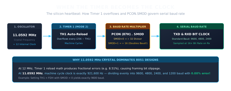
Timer 1 Baud Rate Clock Pipeline
Look closely at PCON (Power Control, 87H).
While PCON is not bit-addressable, its most significant bit is SMOD (Bit 7):
* When SMOD = 0, the baud rate clock divider is 32.
* When software sets SMOD = 1, silicon divides by 16 instead, instantly doubling the serial baud rate without altering Timer 1!
The Mystery of the 11.0592 MHz Crystal
If you examine classic 8051 development boards, you will almost never find a clean 12.000 MHz crystal.
Instead, you find a curiously specific number printed on the silver metal can: 11.0592 MHz.
Why?
In serial communication, both transmitter and receiver must agree on baud rates (such as 9600, 4800, or 2400 bits per second). If the clock drifts by more than 2% to 3%, bit-sampling slides off target, and framing errors corrupt the byte.
Let us trace the division math:
Machine Cycle Frequency = 11.0592 MHz ÷ 12 = 921,600 Hz
Baud Base Clock = 921,600 Hz ÷ 32 = 28,800 Hz
Look at that resulting number: 28,800 Hz.
It divides cleanly by every standard serial baud rate:
* 28,800 ÷ 9600 = 3 → (Set TH1 = 256 - 3 = 253 = FDH)
* 28,800 ÷ 4800 = 6 → (Set TH1 = 256 - 6 = 250 = FAH)
* 28,800 ÷ 2400 = 12 → (Set TH1 = 256 - 12 = 244 = F4H)
* 28,800 ÷ 1200 = 24 → (Set TH1 = 256 - 24 = 232 = E8H)
The division error is 0.00%. Every bit boundary lands on the exact microsecond.
If an engineer uses a 12.000 MHz crystal instead, 9600 baud requires dividing by 3.255—an impossible fractional rollover for an integer counter! The nearest reload value (TH1 = FDH) produces a baud rate of 10,416 baud—an error of 8.51%, which completely destroys serial communication.
The counter we previously studied in isolation has become the conductor of the serial orchestra.
7. The Serial Interrupt Returns
In our previous exploration The 8051 — When Hardware Decides to Interrupt, we mapped the five hardware voices of the 8051.
We noted that the fifth voice was the Serial Port, vectoring to address 0023H in low Program ROM.
Now we can see the full circuit pathway:
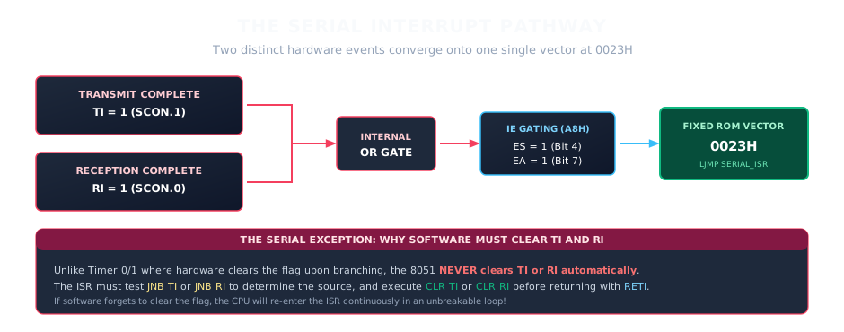
The Serial Interrupt Pathway
TRANSMIT PATH:
Byte shifted out of TXD ────> TI = 1 (SCON.1)
│
├──> OR GATE ────> IE.ES & IE.EA ────> Vector 0023H
│
RECEIVE PATH: │
Byte assembled from RXD ────> RI = 1 (SCON.0)
Two completely distinct physical events feed into a single internal OR gate:
1. When the transmit shift register finishes sending the stop bit, silicon sets TI = 1.
2. When the receive shift register finishes assembling an incoming byte and validates the stop bit, silicon sets RI = 1.
If the serial interrupt is enabled in IE (ES = 1) and the global interrupt breaker is closed (EA = 1), either event diverts the CPU to vector address 0023H.
The Crucial Silicon Asymmetry
Recall the lesson from our Interrupt exploration:
When the CPU vectors to 000BH for Timer 0, hardware automatically clears TF0.
For the Serial Port, hardware NEVER clears TI or RI automatically.
Because both transmission and reception share vector 0023H, the CPU has no way of knowing in hardware which event triggered the jump. Did an outgoing character finish, or did a new character arrive?
The programmer's service routine must resolve the question in software:
SERIAL_ISR:
JNB RI, CHECK_TI ; Did a byte arrive? If not, check transmit
MOV A, SBUF ; Read incoming byte from SBUF receive latch
CLR RI ; MUST MANUALLY CLEAR RI IN SOFTWARE!
; Process incoming data...
CHECK_TI:
JNB TI, ISR_EXIT ; Did a transmission complete?
CLR TI ; MUST MANUALLY CLEAR TI IN SOFTWARE!
; Load next character into SBUF if available...
ISR_EXIT:
RETI ; Pop PC, restore priority status flip-flop
If the developer forgets to execute CLR TI or CLR RI, the moment RETI executes, the active flag will immediately pull the interrupt line low again, trapping the processor in an inescapable interrupt loop.
8. The Complete 8051 Serial Conversation
Step back and look at the entire serial landscape:
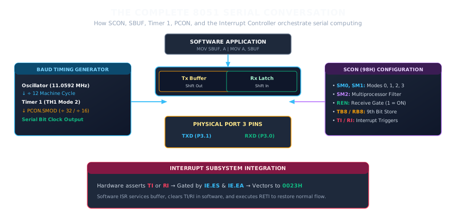
The Complete 8051 Serial Architecture
The serial port of the 8051 is not simply "pins 10 and 11 on the DIP package."
It is a coordinated, multi-peripheral machine:
1. The Software Layer communicates through a single address: SBUF (99H).
2. The Dual Buffer Architecture splits writes to the Transmit Shift Register and reads from the Receive Latch, guaranteeing full-duplex operation.
3. The Timing Engine borrows Timer 1 in Mode 2, dividing an 11.0592 MHz crystal through PCON.SMOD to generate standard baud rates with zero drift.
4. The Control Surface in SCON steers internal multiplexers between synchronous shift register expansion (Mode 0), standard 8-bit UART (Mode 1), and 9-bit multiprocessor bus networks (Modes 2 and 3).
5. The Protocol Arbiter (SM2) filters out unaddressed traffic in hardware, preserving CPU cycles on multi-drop buses.
6. The Interrupt Subsystem ties TI and RI through IE.ES to vector 0023H, alerting software the instant the hardware finishes speaking or hearing.
9. The Deeper Realization
The 8051 serial port was never just TXD and RXD.
Behind those two pins sits a miniature communication ecosystem.
Look at the architectural division of responsibility:
SCON Decides HOW the machine speaks (Mode, Framing, SM2, REN).
SBUF Carries WHAT the machine says (Dual-register data gateway).
Timer 1 / PCON Determines HOW QUICKLY the machine speaks (Baud rate heartbeat).
TXD / RXD Forms the PHYSICAL MEDIUM (Port 3 pins touching the wire).
TI / RI Tells the machine THAT AN EVENT OCCURRED (Status flags).
IE (ES / EA) Decides WHETHER THE CPU LISTENS (Gated interrupt authority).
ISR / RETI EXECUTES THE RESPONSE and resets the silicon lock.
The beauty of the classic 8051 is not that it had the fastest serial port, nor the largest buffers.
Its brilliance lay in how few silicon gates it required to build a complete communication system:
* It did not require a dedicated baud rate oscillator—it shared Timer 1.
* It did not require separate read and write addresses—it mapped both to SBUF.
* It did not require an external network controller—it embedded multiprocessor address filtering into SM2 and the 9th bit.
Software defines the policy. Hardware conducts the rhythm.
And across two humble pins, the controller learns to speak to the world.
Current Exploration
The 8051 — When the Controller Learns to Speak
Next →
None