Controller
The 8051 — When Time Becomes a Signal
How the classic 8051 specializes the architecture of hardware timing through its Special Function Registers.
Controller8051MicrocontrollerTimersCountersHardware TimingTCONTMODEmbedded Systems
1. The Doors We Left Unopened
In our exploration of the 8051 Special Function Register map, we walked through the upper data space above 7FH.
We saw how Intel's architects mapped the entire machine—CPU registers, parallel I/O ports, serial communications, and interrupt controls—into a unified control surface. And right in the middle of that map, six registers appeared under a single heading:
TIMERS & COUNTERS
│
├── TCON (88H) → Timer / Counter Control Register (Bit-Addressable)
├── TMOD (89H) → Timer / Counter Mode Register (Byte-Only)
│
├── TL0 (8AH) → Timer 0 Low Byte
├── TL1 (8BH) → Timer 1 Low Byte
├── TH0 (8CH) → Timer 0 High Byte
└── TH1 (8DH) → Timer 1 High Byte
In that previous exploration, these registers were only addresses—quiet names on a silicon layout, closed doorways sitting on the machine's control surface.
Now we can open them.
2. Concrete Silicon, Not Abstract Theory
In the Coordination node of the PrajnaEdge Tree, our exploration The Architecture of Time established the universal grammar of machine timing:
Clock Source ───► Counter ───► Overflow ───► Event
We saw that to break free from the trap of CPU software delay loops—where the processor burns millions of cycles spinning in empty decrement loops, blind to the outside world—a machine must delegate time to autonomous digital counting circuits.
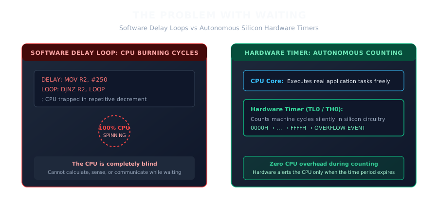
Software Delay Loop vs Autonomous Hardware Timer
That was the universal concept.
But abstract concepts do not execute on circuit boards. Real silicon does.
Now let us step out of theory and look into one actual, historical machine. How does the classic Intel 8051 actually implement this timing architecture?
In the 8051, there are no generic auto-reload registers, no multichannel capture-compare complexes, and no complex bus arbitration layers. Instead, the 8051 gives the universal timing model a lean, concrete form:
8051 Oscillator / 12 ───► Timer 0 / 1 ───► THx:TLx ───► TFx Flag ───► CPU / ISR Action
The entire mechanism is operated through the six Special Function Registers we met in the memory map.
3. The Clock Is Already Moving
Where does an 8051 get its time?
It does not generate time out of nothing. The moment power is applied to the chip, an external quartz crystal begins oscillating—traditionally at 12 MHz.
Inside the chip, frequency divider circuits partition this oscillation into machine cycles. In the classic 8051, exactly 12 oscillator periods form one machine cycle:
Machine Cycle Frequency = 12 MHz / 12 = 1 MHz
1 Machine Cycle = 1 µs
This rhythm is already flowing. Every instruction fetch, every memory cycle, and every bus operation beats to this steady, relentless 1-microsecond pulse train.
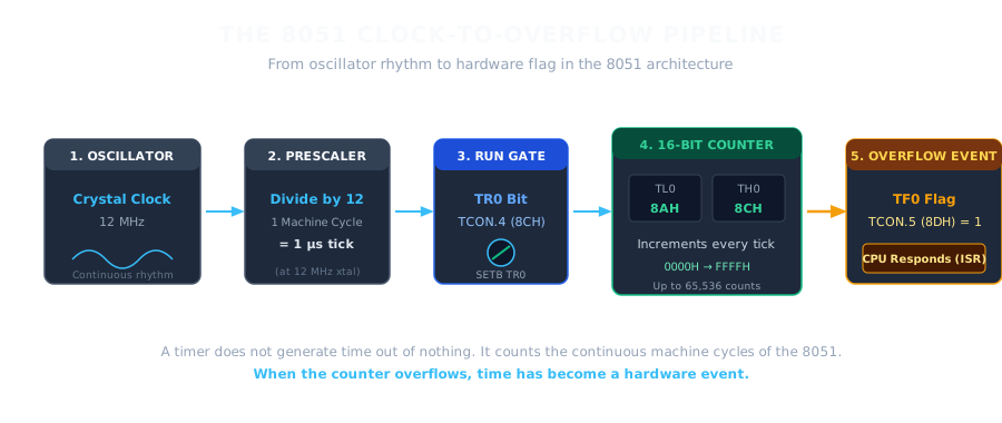
The 8051 Clock-to-Overflow Pipeline
The 8051 timer does not create a new clock. It simply taps into this preexisting stream of machine cycles, passes it through a software-controlled run gate (TR0), and feeds it into an autonomous 16-bit counting register (TH0:TL0).
While software executes instructions elsewhere, the counter increments on every cycle in silence.
4. Timer or Counter? The C/T Decision
Here we arrive at an essential architectural realization.
What is the fundamental difference between measuring time and counting external events?
To a programmer, they feel like two completely different tasks:
- Measuring time means waiting for 50 milliseconds to elapse.
- Counting events means tallying revolutions of an optical motor encoder or recording sensor pulses on a factory belt.
Yet to digital hardware, both operations are identical:
Pulses Arrive ───► Counter Register Increments by 1
The 8051 does not duplicate silicon by building two separate subsystems for timers and counters. It uses the exact same 16-bit counting hardware for both.
All that changes is where the pulses come from:
1. Timer Mode (C/T = 0):
The counter is fed by the internal machine cycle clock (Oscillator / 12). Because pulses arrive at regular, predictable intervals, the accumulated count directly represents elapsed time.
2. Counter Mode (C/T = 1):
The counter is disconnected from the internal clock and connected directly to an external chip pin:
- Pin P3.4 (T0) for Timer 0
- Pin P3.5 (T1) for Timer 1
Whenever a 1-to-0 negative electrical transition occurs on the pin, the hardware increments the register. The counter is now counting physical happenings in the outside world.
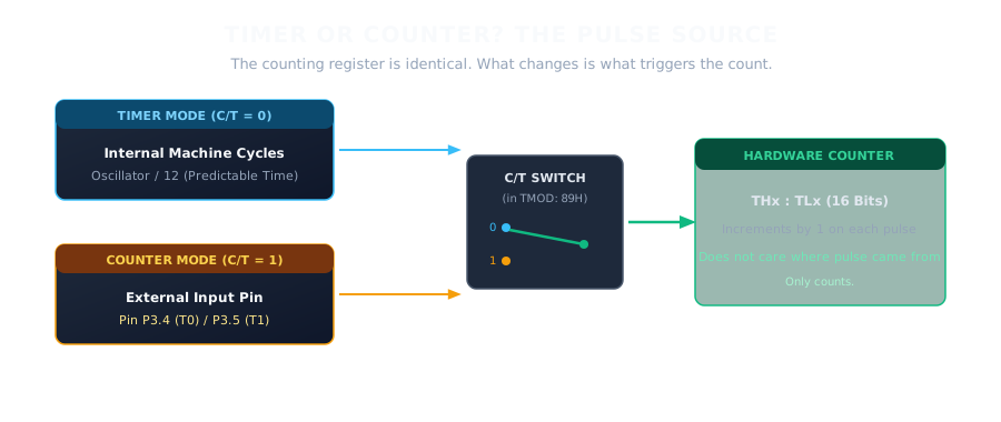
Timer or Counter? The Pulse Source
The selector switch between these two modes is a single bit in silicon: the C/T bit in TMOD (89H).
5. Two Timers, One Architectural Pattern
The 8051 contains two identical, independent timing blocks: Timer 0 and Timer 1.
Let us observe how their physical counting registers are paired in hardware:
The 16-Bit Counter Pairings
A classic 8051 CPU operates on an 8-bit internal data bus. To count up to 65,535, each 16-bit timer is split across two separate 8-bit Special Function Registers:
TIMER 0 — 16-BIT HARDWARE COUNTER
Max: 65,535 (FFFFH)
TH0 (8CH)
High Byte • Bits 15..8
TL0 (8AH)
Low Byte • Bits 7..0
Bit 15
← Cascading 16-bit Count Range →
Bit 0
TIMER 1 — 16-BIT HARDWARE COUNTER
Max: 65,535 (FFFFH)
TH1 (8DH)
High Byte • Bits 15..8
TL1 (8BH)
Low Byte • Bits 7..0
Bit 15
← Cascading 16-bit Count Range →
Bit 0
Notice the pairing in the SFR address space:
- The low bytes are placed adjacent at 8AH (TL0) and 8BH (TL1).
- The high bytes are placed adjacent at 8CH (TH0) and 8DH (TH1).
Together, TL0 and TH0 form a 16-bit digital register capable of counting from 0000H up to FFFFH (65,535 counts). TL1 and TH1 form an identical 16-bit register for Timer 1.
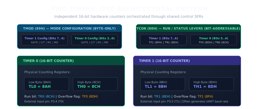
Two Timers, One Architectural Pattern
Both timers operate completely independently, yet both are supervised through two shared registers: TMOD and TCON.
6. The Control Panel: TMOD vs TCON
Why did Intel's architects split timer control across two separate registers instead of one?
Recall the bit-addressable rule from The 8051 — Where Software Touches Hardware:
An SFR is bit-addressable if and only if its address ends in 0H or 8H.
This rule reveals the profound architectural divide between setting rules and pulling live levers:
TMOD (89H): Setting the Rules Once
Address 89H does not end in 0H or 8H. It is byte-only.
TMOD is configured during system boot to establish operating policies:
- Is Timer 0 operating as a Timer (C/T = 0) or Counter (C/T = 1)?
- What is its counting structure (M1, M0): 13-bit Mode 0, 16-bit Mode 1, or 8-bit Auto-Reload Mode 2?
- What are the corresponding policies for Timer 1?
Because configuration is written once during setup, bit-by-bit manipulation is unnecessary. Here is how TMOD is organized in silicon:
TMOD (89H) — TIMER / COUNTER MODE REGISTER
BYTE-ONLY • RESET: 00H
Bit 7Bit 6Bit 5Bit 4Bit 3Bit 2Bit 1Bit 0
← TIMER 1 CONFIGURATION (Bits 7..4) →
← TIMER 0 CONFIGURATION (Bits 3..0) →
Software writes the whole byte during initialization:
MOV TMOD, #01H ; Timer 0 in 16-bit Timer Mode (C/T = 0, Mode 1)
TCON (88H): The Live Operational Levers
Address 88H ends in 8H. It is bit-addressable!
TCON contains the live runtime switches and status flags that software must touch constantly:
TCON (88H) — TIMER / COUNTER CONTROL REGISTER
BIT-ADDRESSABLE • RESET: 00H
Bit 7Bit 6Bit 5Bit 4Bit 3Bit 2Bit 1Bit 0
TIMER 1 (TF1, TR1)
TIMER 0 (TF0, TR0)
EXTERNAL INTERRUPTS (INT1, INT0)
- TR0 (8CH) / TR1 (8EH) — Timer Run Bits:
The run gates. When TR0 = 0, pulses are blocked and the counter freezes. When TR0 = 1, pulses flow into the counter. Because TCON is bit-addressable, software starts or stops counting with a single atomic instruction:
SETB TR0 ; Open gate: Timer 0 begins counting
CLR TR0 ; Close gate: Timer 0 halts immediately
- TF0 (8DH) / TF1 (8FH) — Timer Overflow Flags:
The alert signals. When the counter rolls over from its limit back to 0000H, the hardware automatically sets TF0 = 1. This flag announces to the CPU that the allotted time or pulse tally has completed.
7. The Boundary: Autonomous Hardware and CPU Response
Here we observe the precise architectural division between hardware execution and software responsibility.
The timer does not burden the processor with counting individual pulses. Hardware handles the mechanical accumulation entirely on its own:
[1. AUTONOMOUS HARDWARE]
Clock or Pin Pulses ──► Increment THx:TLx in silicon
↓
Counter reaches capacity and rolls over (e.g. FFFFH → 0000H)
↓
Hardware asserts overflow flag: TFx = 1 (in TCON)
[2. CPU / SOFTWARE RESPONSE]
CPU detects TFx = 1 (via polling loop or Interrupt Service Routine)
↓
Software performs deliberate application task
↓
Software acknowledges event: CLR TFx
Hardware does what hardware does best: precise, deterministic, relentless counting without spending CPU cycles.
Software does what software does best: interpreting the event and deciding how the broader machine should respond.
8. The Deeper Realization
The classic 8051 does not require its central processor to count every passing moment.
Instead of chaining the CPU to an empty loop of decrements and checks, the architecture provides a dedicated counting mechanism in silicon.
The relationship is clean and deliberate:
Software establishes the rules inside TMOD.
The clock supplies the rhythm.
The counter registers (THx and TLx) accumulate counts in silence.
And TCON presents the live surface—allowing software to start the process with a single bit, pause it at will, and notice the exact instant when an interval expires.
By separating the measurement of time from the execution of instructions, the 8051 transforms an intangible physical flow into an organized, observable hardware event. Time is no longer something software must wait for—it has become a resource software can configure, measure, and command.
Current Exploration
The 8051 — When Time Becomes a Signal