Controller
Inside the 8051
Opening the classic microcontroller to explore its central processing core, internal memories, Special Function Registers, and peripheral subsystems.
Controller8051MicrocontrollerArchitectureCPUSFRHardwareEmbedded Systems
1. Open the Chip
We've seen why the 8051 mattered.
It brought computation, memory, timing, communication, and digital I/O onto a single die, proving that a computer didn't have to sit beside a machine — it could become part of the machine.
But knowing that it contains a CPU, memory, ports, timers, and communication hardware is only the beginning.
Where exactly are these pieces?
How does the CPU interact with them?
Where does the program live?
Where does the data go?
And what are all those registers actually doing?
Let's open the 8051.
Before looking beneath the plastic packaging, we first encounter the boundary where the microcontroller meets the outside world: its physical pins.
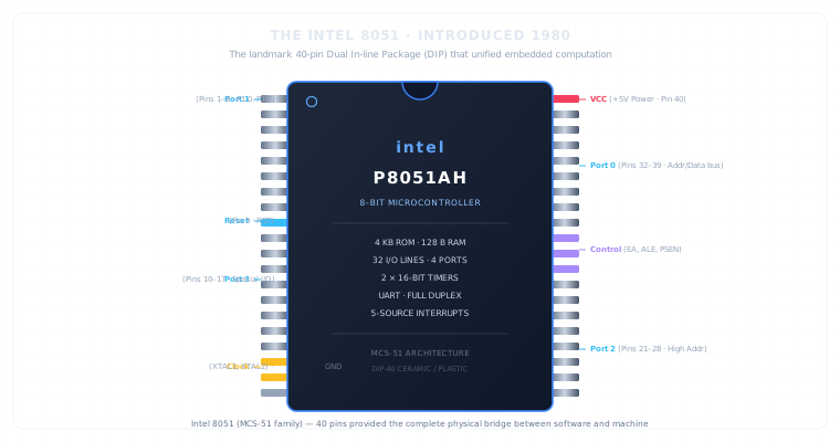
The Intel 8051 40-Pin DIP Package
The classic 8051 is housed in a standard 40-pin Dual In-line Package (DIP).
These forty metal pins are the physical interface between the silicon die inside and the external electrical circuit. Through them, the chip draws power, senses signals from buttons and sensors, asserts control voltages to relays and motors, and exchanges serial data with other machines.
Before we look inside the chip, we can see how the chip meets the outside world.
2. From Pins to the Machine Inside
The pins, however, are only the boundary.
Inside the package sits a complete, coordinated computing system. When we step past the physical leads and look at the silicon layout, the collection of pins resolves into a structured architectural map.
40-pin physical package
↓
internal architecture
Every pin connects back to an internal functional block: a port latch, a power rail, an oscillator circuit, or a control line.
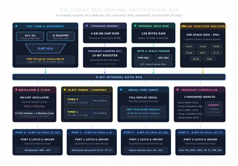
The Classic 8051 Internal Architectural Map
At the heart of the 8051 is a unified architectural structure:
CPU
↓
memory / registers
↓
peripherals
↓
I/O pins
Running through the center of the chip is an 8-bit internal data bus. This shared highway connects the central processing unit, the on-chip program memory, the internal data RAM, the Special Function Registers, the hardware timers, the serial interface, and the four parallel I/O ports.
Understanding the 8051 means understanding how these major functional blocks divide the work of machine control.
3. The CPU at the Center
At the center of the architecture sits the Central Processing Unit (CPU). It fetches instructions, decodes opcodes, performs mathematical and logical computations, and directs data movement across the internal bus.
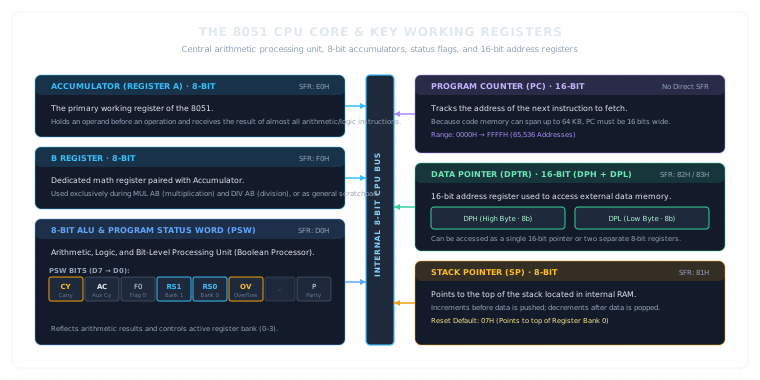
The 8051 CPU Core and Primary Working Registers
The 8051 CPU is organized around several primary registers, each engineered for a distinct functional role:
- Arithmetic Logic Unit (ALU): An 8-bit computational engine that performs binary addition, subtraction, multiplication, division, and logical operations (AND, OR, XOR), as well as bit-level boolean manipulations.
- Accumulator (Register A): The primary 8-bit working register used extensively across the instruction set. The ALU typically takes one of its operands from the Accumulator and writes the computational result directly back into it.
- B Register: An 8-bit register used primarily in tandem with the Accumulator during hardware multiplication (MUL AB) and division (DIV AB) instructions. When not performing arithmetic, it serves as a general-purpose register.
- Program Counter (PC): A 16-bit register that keeps track of the memory address of the next instruction to be fetched from program memory. Because the 8051 architecture supports up to 64 KB of code space, the PC requires a full 16-bit width.
- Data Pointer (DPTR): A 16-bit register composed of two 8-bit registers (DPH and DPL). It serves primarily as an address pointer to access external data memory and lookup tables.
- Program Status Word (PSW): An 8-bit register containing arithmetic status flags (Carry, Auxiliary Carry, Overflow, Parity) that reflect the result of recent ALU operations, as well as control bits that select the active register bank.
- Stack Pointer (SP): An 8-bit register that points to the current top of the stack located within internal RAM.
These registers form the core execution engine of the 8051. Together, they allow the processor to calculate, maintain state, and traverse instructions.
4. Where the Program Lives
A microcontroller cannot function without instructions telling it what to do. In the 8051, those instructions live in Program Memory.
Program Memory → instructions / code
The classic 8051 features 4 KB of on-chip Read-Only Memory (ROM), which occupies addresses 0000H through 0FFFH. This memory holds the compiled firmware instructions permanently, retaining code even when power is disconnected.
Key architectural characteristics of the program memory system include:
- 16-Bit Addressing Space: The 8051's Program Counter is 16 bits wide, allowing the architecture to address a total of 64 KB (216 = 65,536 bytes) of program memory.
- Internal and External Code: While the original 8051 contains 4 KB on-chip, the memory structure allows seamless expansion to external program memory up to the full 64 KB limit.
- Dedicated Execution Path: In accordance with the Harvard architecture model, program instructions reside in their own dedicated address space, physically and logically isolated from data storage.
When the 8051 powers up or resets, the Program Counter initializes to address 0000H, and the CPU begins fetching its first instruction.
5. Where the Data Lives
While program memory stores the static instructions of the firmware, a microcontroller also requires memory to store dynamic runtime information: sensor readings, calculation results, state flags, and function return addresses.
In the 8051, data memory is divided into two fundamentally different spaces: Internal RAM and Special Function Registers (SFRs).
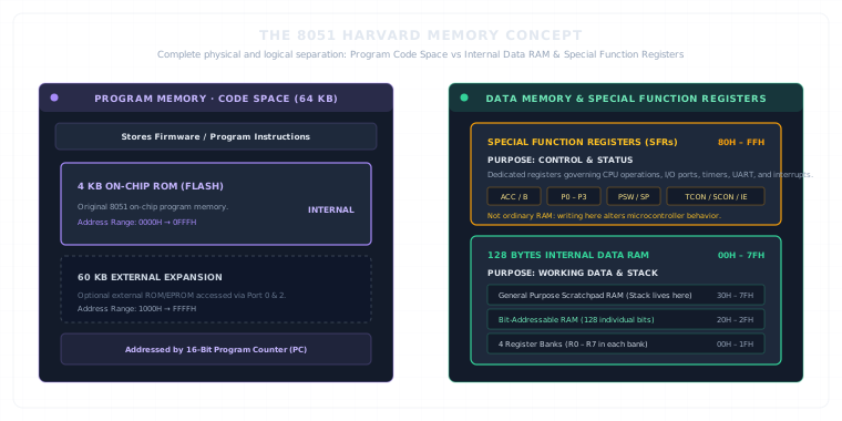
The 8051 Harvard Memory Concept
Internal Data RAM (128 Bytes)
The classic 8051 contains 128 bytes of high-speed internal static RAM occupying addresses 00H through 7FH.
This memory space serves several distinct roles:
- Register Banks: The lowest 32 bytes (00H–1FH) are organized into four separate banks of eight working registers each (R0 through R7).
- Bit-Addressable RAM: The next 16 bytes (20H–2FH) provide 128 individually addressable bit locations, allowing single-bit flags to be manipulated without disturbing adjacent data.
- General-Purpose Scratchpad: The remaining bytes (30H–7FH) provide general-purpose variable storage.
- The System Stack: Unlike many general-purpose microprocessors where the stack resides in external memory, the 8051 stack lives directly inside internal RAM.
Special Function Registers (SFRs)
Above the 128 bytes of general RAM sits an entirely distinct functional domain: the Special Function Register (SFR) space (addresses 80H through FFH).
SFRs are not ordinary memory locations for storing variables. Instead, they are the hardware control and status registers for the entire microcontroller.
Internal RAM → working data
SFRs → control and status of the CPU and peripherals
Writing a byte to internal RAM simply saves a value for later retrieval. But writing a byte to an SFR configures a hardware timer, changes a port pin voltage, alters an interrupt priority, or initiates serial transmission.
Through SFRs, the CPU directs and monitors every peripheral inside the chip:
- CPU Control: Accumulator (A), B, PSW, SP
- I/O Ports: P0, P1, P2, P3
- Timers: TCON, TMOD, TL0, TH0, TL1, TH1
- Serial Communication: SCON, SBUF
- Interrupts & Power: IE, IP, PCON
Separating working data RAM from hardware-governing SFRs is one of the defining organizational principles of the 8051 architecture.
6. The Peripherals Around the CPU
Surrounding the central CPU core and memories are dedicated on-chip peripheral circuits. These hardware blocks offload time-critical tasks from the processor, allowing the 8051 to interact directly with the physical world.
Four 8-Bit Parallel I/O Ports
The 8051 provides 32 digital input/output pins divided into four 8-bit parallel ports:
- Port 0 (P0.0–P0.7)
- Port 1 (P1.0–P1.7)
- Port 2 (P2.0–P2.7)
- Port 3 (P3.0–P3.7)
Each port consists of an internal latch and driver circuit mapped to a corresponding SFR. All four ports are bi-directional. While Port 1 serves primarily as dedicated general-purpose digital I/O, Ports 0, 2, and 3 serve alternate hardware functions when interfacing with external memories, interrupts, timers, or serial lines.
Timers / Counters
The 8051 includes two independent 16-bit timer/counter blocks:
- Timer 0
- Timer 1
Each timer is composed of two 8-bit registers (High and Low bytes). In timer mode, the block counts internal clock pulses to measure precise time intervals or generate regular periodic events. In counter mode, the block counts negative transitions on external pins (T0 and T1) to track external events such as pulse trains or revolution sensors.
Serial Port (UART)
Built directly into the silicon die is a full-duplex universal asynchronous receiver/transmitter (UART).
The serial port allows the 8051 to transmit and receive serial data simultaneously over two dedicated pins: Receive Data (RxD on P3.0) and Transmit Data (TxD on P3.1). The CPU reads and writes serial data through the SBUF register, while configuring baud rates, framing, and modes through SCON.
Interrupt Controller
A control system must be able to respond immediately to critical real-world occurrences. The 8051 incorporates a hardware interrupt system capable of managing five distinct interrupt sources:
- Two external hardware interrupts (/INT0 and /INT1)
- Two internal timer overflow interrupts (Timer 0 and Timer 1)
- One internal serial communication interrupt (Transmit/Receive complete)
When an enabled interrupt occurs, the controller automatically suspends the main program execution, preserves the Program Counter, and vectors directly to a dedicated Service Routine. This allows the 8051 to react swiftly to urgent external events without wasting processing power in continuous polling loops.
7. The Clock That Keeps It Moving
None of these internal blocks can function without a heartbeat.
The classic 8051 contains an on-chip oscillator circuit that works with an external quartz crystal, ceramic resonator, or clock source connected between pins XTAL1 and XTAL2 to generate its fundamental operating frequency.
A 12 MHz crystal is the classic benchmark frequency commonly associated with the original 8051, but the oscillator frequency is not inherently fixed at 12 MHz. Different applications and later 8051 variants operate across a wide range of frequencies, from low-power kilohertz clocks up to tens of megahertz.
12 Oscillator Periods = 1 Machine Cycle
In the classic 8051 architecture, timing is structured around a 12-clock cycle model:
- The oscillator generates continuous clock pulses.
- Twelve consecutive oscillator pulses form one machine cycle.
- The CPU executes simple instructions in one or two machine cycles.
Because of this 12-to-1 relationship, an 8051 running on a 12 MHz crystal completes exactly one machine cycle in 1 mus (one microsecond). This predictable relationship provided engineers with straightforward, deterministic timing calculations for control loops and delays.
8. One Machine, Many Blocks
When we step back and examine the complete 8051, we see that it is not merely a central processor with some peripheral modules attached to its pins.
It is a single, tightly coordinated control pipeline:
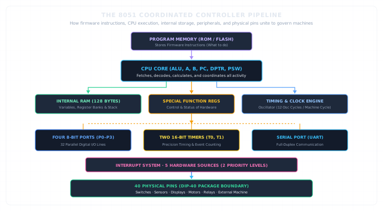
The 8051 Coordinated Controller Pipeline
PROGRAM MEMORY
↓
CPU
↙ ↓ ↘
RAM SFRs CONTROL
↓
┌──────────┼──────────┐
↓ ↓ ↓
PORTS TIMERS SERIAL
↓ ↓ ↓
INTERRUPTS
↓
I/O PINS
↓
PHYSICAL WORLD
The flow is deliberate and direct:
1. Firmware in Program Memory instructs the CPU on how to behave.
2. The CPU Core processes instructions, manipulates data in Internal RAM, and governs peripherals through the Special Function Registers (SFRs).
3. The Peripherals (Ports, Timers, Serial UART) generate timing, monitor communication, and interact with the Interrupt System.
4. The Physical Pins interface these signals directly with external sensors, switches, displays, and actuators.
Every block exists to support the mission of embedded control: observing physical conditions, evaluating logic, and enforcing timely physical actions.
9. The Architecture Is Now Open
We can now see the 8051 as a complete machine.
The CPU performs the computation.
Program memory holds the instructions.
RAM holds working data.
SFRs control and report the state of the system.
Ports connect it to the outside world.
Timers measure and generate time-based events.
The serial interface allows communication.
Interrupts allow the CPU to respond to important events.
But seeing the architecture is only the beginning.
Where exactly does all that memory live?
How are the 128 bytes of RAM organized?
Where do the register banks sit?
Which locations are bit-addressable?
And where do the SFRs fit into the memory map?
That is where we go next.
Current Exploration
Inside the 8051