Coordination
When Machines Learned to Speak Back
How numbers became reality.
DACR-2R LadderPWMReconstruction FilterWaveform Generation
1. The Need to Influence Reality
Sensing the world is a passive act. A microcontroller can read an ADC, clocking timing intervals and translating physical temperatures, light levels, or voltages into neat digital variables. But observation alone does not change the physical state of a system. A machine that can only observe is a brain trapped in a jar—fully aware of its environment but powerless to act.
To become purposeful, a machine must eventually influence its surroundings. It needs to drive a speaker cone to vibrate air and generate sound, adjust the speed of a high-torque motor in an industrial conveyor, produce a specific reference voltage to calibrate another sensor, or generate a precise high-frequency carrier wave for radio transmission. Every active control system, from a simple thermostat to a multi-axis surgical robot, requires the ability to write actions back into physical space. Observation must give way to influence.
2. The Reverse Journey
This requirement defines a symmetrical engineering challenge. In our earlier explorations, we watched the Analog-to-Digital Converter (ADC) carve physical reality into discrete digital states. The ADC took a continuous voltage, sampled it at discrete intervals in time, and rounded it to the nearest binary code on a grid. It was a journey from continuous physics to discrete numbers.
To speak back, the machine must take the reverse journey. It must start with a discrete binary code—a neat integer stored in a CPU register—and translate it back into a continuous physical voltage. This is the domain of the Digital-to-Analog Converter (DAC). Below is a conceptual representation of this symmetry:
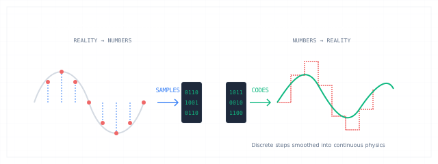
The Symmetry of ADC and DAC pathways
Figure 1: While the ADC slices continuous signals into discrete digital numbers, the DAC maps numbers back into physical voltages.
3. How a DAC Works: The Resistor Divider Intuition
How does a chip translate an abstract binary number into a real physical voltage? At its heart, a DAC is a network of resistors and switches that divide a stable Reference Voltage ($V_{REF}$) down to a specific fraction.
Consider a simple resistor divider ladder. A binary code represents a set of instructions for a switch matrix. For instance, in a classic R-2R ladder architecture, each bit of the digital input code controls a corresponding physical switch. If a bit is 1, its switch connects a node in the resistor ladder to the Reference Voltage ($V_{REF}$). If a bit is 0, the switch connects that node to ground. The current splits symmetrically at each R-2R junction. By summing these scaled currents, the DAC generates an output current directly proportional to the digital code, which is then buffered by an operational amplifier to output a clean, stable voltage. The hardware block diagram below illustrates this pipeline:
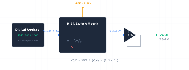
DAC Pipeline Block Diagram
Figure 2: The internal elements of a DAC: input register, switch matrix, resistor scaling network, and output buffer.
4. Resolution: Slicing the Staircase
Just as with ADCs, a DAC's precision is governed by its Resolution. Resolution defines the number of discrete steps the DAC can use to construct its output voltage.
- An 8-bit DAC yields $2^8 = 256$ discrete voltage steps.
- A 10-bit DAC provides $2^{10} = 1024$ steps.
- A 12-bit DAC provides $2^{12} = 4096$ steps, which is standard for high-quality microcontroller peripherals.
- A 16-bit DAC provides $2^{16} = 65,536$ steps, used in high-fidelity audio equipment where stepped jaggedness would introduce audible distortion.
The smallest voltage change the DAC can output is called the Least Significant Bit (LSB) size. As resolution increases, the step size shrinks, transforming a coarse, jagged staircase into a smooth line. Below is a comparison of output granularity across resolutions:
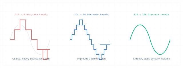
DAC Resolution Step Comparison
Figure 3: High resolution minimizes the quantization step size, allowing the DAC to reconstruct curves with minimal distortion.
5. Reference Voltage: The Boundary Ruler
A DAC cannot output a voltage larger than the Reference Voltage ($V_{REF}$) supplied to its core. $V_{REF}$ acts as the physical ruler that calibrates the digital steps. The relationship between the output voltage ($V_{OUT}$), the digital code, the resolution ($N$), and $V_{REF}$ is defined as:
$V_{OUT} = V_{REF} \times \frac{\text{Digital Code}}{2^N - 1}$
If $V_{REF}$ is 3.3V, a 12-bit code of 4095 outputs exactly 3.3V, while 2048 outputs 1.65V. If $V_{REF}$ drifts or contains high-frequency electrical noise, that noise couples directly into $V_{OUT}$—if the ruler expands and contracts, the measurements scale with it. Therefore, a clean, stable, and decoupled reference voltage is vital for analog precision. Below is an illustration of how $V_{REF}$ defines the output scaling boundaries:
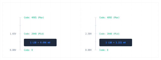
Reference Voltage Scaling
Figure 4: Reference voltage dictates both the maximum output range and the individual step size (LSB) of the converter.
6. Waveform Generation: Building Curves from Steps
To generate a dynamic waveform—such as a smooth audio tone, a linear motor ramp, or a calibration pulse—the CPU writes a continuous stream of digital values to the DAC register in a periodic loop driven by timer interrupts.
For example, to generate a Sine Wave, engineers compute a table of sine values beforehand and load them into memory. Every time a timer overflows, a DMA (Direct Memory Access) channel automatically copies the next value from the table directly into the DAC data register without CPU intervention. By updating the DAC at a high, constant frequency, the discrete steps approximate a continuous curve. The illustrations below depict how different waveforms are constructed by sequencing discrete values:
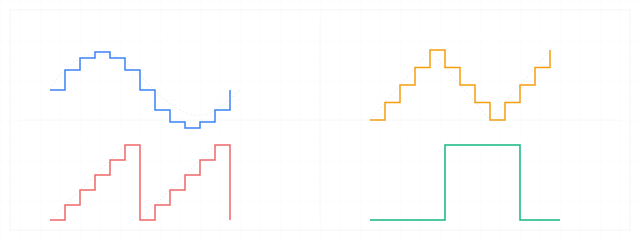
Waveform Generation
Figure 5: Building Sine, Triangle, Sawtooth, and Square waveforms by outputting timed sequences of digital codes.
7. The Illusion of Continuity: Filtering the Steps
If you look closely at a raw DAC output on an oscilloscope, you will see a stair-step pattern. If this raw voltage is fed directly to a high-frequency speaker, the sharp corners of the steps (which represent high-frequency harmonic distortion) will cause an audible hiss or crackle. How do we turn these steps into a truly smooth curve?
The solution is a Reconstruction Filter. This is a low-pass analog filter placed immediately after the DAC output pin. A simple resistor-capacitor (RC) filter removes the high-frequency transitions (the sharp corners of the steps), leaving only the fundamental low-frequency analog wave. Furthermore, many physical loads (like speaker diaphragms or heavy motor coils) possess natural mechanical or inductive inertia, meaning they cannot react instantly to the steps anyway. They act as natural low-pass filters, integrating the steps into smooth physical movements. Below is a diagram of low-pass reconstruction filtering:
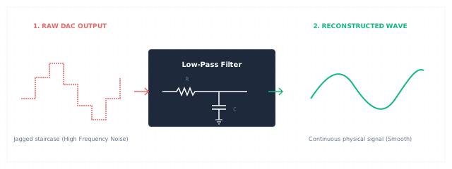
Low-Pass Reconstruction Filter
Figure 6: A low-pass filter integrates the sharp steps of the raw DAC output, smoothing it into a continuous analog waveform.
8. PWM: The Impostor DAC
In many embedded systems, dedicated DAC hardware is absent because it requires substantial PCB silicon and pin counts. Instead, engineers often use a timer to generate Pulse-Width Modulation (PWM) signals, mimicking an analog output.
By toggling a digital pin rapidly between 0V and 3.3V at a high frequency (often tens of kilohertz) and adjusting the Duty Cycle (the ratio of HIGH time to the total period), we can represent different voltages. If we pass this PWM stream through a low-pass RC filter, the filter integrates the square pulses, smoothing the high-frequency switching into a steady DC voltage directly proportional to the duty cycle. The diagram below illustrates this integration:
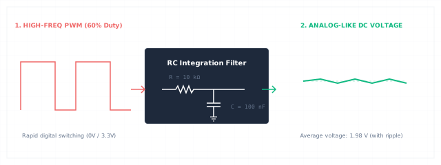
PWM Impostor DAC
Figure 7: Using high-frequency PWM duty-cycle pulses combined with a low-pass filter to generate an average analog voltage.
While PWM is cheap, simple, and highly efficient for power applications (like driving LEDs or brushless motors), it is an imperfect 'impostor' DAC. It suffers from slow response times (due to filter charging delays) and contains switching ripple noise that is difficult to filter out completely. A true DAC provides a steady, immediate voltage level without switching noise. The comparison below contrasts the two methods:
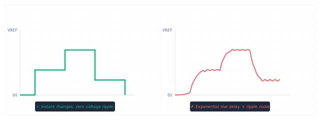
PWM vs True DAC Comparison
Figure 8: A true DAC provides clean, instantaneous voltage steps, whereas a filtered PWM introduces exponential rise delays and ripple noise.
9. Painting with Voltage
Let's observe these conversion behaviors. In the interactive panel below, modify reference voltage, DAC resolution, and digital input codes to watch how digital values translate into analog voltages on a meter.
10. The Illusion of Smoothness
How does sequence timing and low-pass filtering shape the output waveform? In the simulator below, adjust the waveform type, update rate, resolution, and low-pass reconstruction filter cutoff to see how a continuous curve is painted.
11. Real Embedded Applications
DACs are the expressive voice of microcontrollers. They drive audio amplifiers in smart speakers, generate control voltages in industrial loops (like proportional valves), produce high-frequency diagnostic test signals in lab instruments, calibrate medical pacemakers, and execute motor speed profiling in robotics. By giving digital systems a path to write back to the physical world, the DAC completes the handshake between computational logic and physical reality.
The Expressive Handshake
Timers taught machines when to pay attention. ADCs taught machines how to translate reality into digital coordinates. DACs taught machines how to write numbers back into physical reality.
For the first time, a machine could not only understand its environment, but actively influence it. Yet as these sensory and output capabilities expanded, a new system challenge emerged. Managing high-speed sampling, responding, keeping time, and communicating all at once required synchronized scheduling. The next engineering frontier was no longer sensing or speaking—it was scheduling what deserved the processor's attention next.
A processor without a DAC is a mind without a voice—fully capable of thought, but unable to sing.
Current Exploration
When Machines Learned to Speak Back