PrajnaEdge
An interactive engineering platform where complex concepts become experiences—through visual explorations, simulations, and practical understanding.
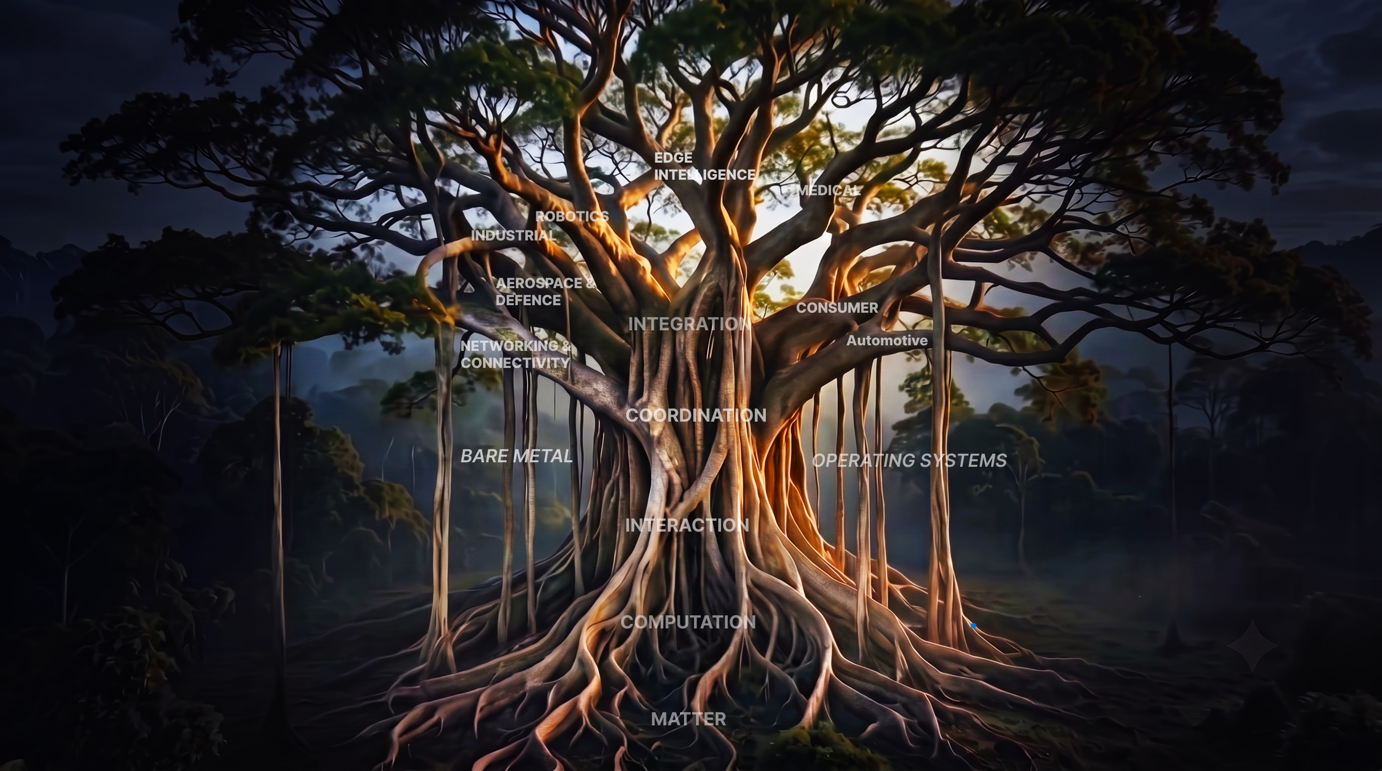
PrajnaEdge Navigation Tree
Embedded Systems Tree
On the Horizon
PravahaPath
Something new is taking shape.

Articles & Write-ups

Exploring how systems evolve from hardware to integration.

Sort:

Edge AI Demonstrations

Deploying neural networks and intelligent decision loops on raw silicon targets.

Sort:
Computation

The Architecture of Memory

How physical constraints and electrical charge define the boundaries of digital state.

MemorySRAMDRAMFlashEmbedded Systems

1. The Hierarchy of State

Every processor is fundamentally a state machine. It executes instructions by reading data from memory, transforming it, and writing it back. But not all memory is created equal. The physical reality of silicon forces a compromise between speed, capacity, and cost.

To build a useful system, we construct a hierarchy: registers and SRAM at the very top (tapering down near the CPU core for speed), backed by main DRAM system memory, and finally persistent NOR and NAND flash for mass storage. This tiered architecture ensures the CPU is never starved of instructions while keeping persistent data accessible.
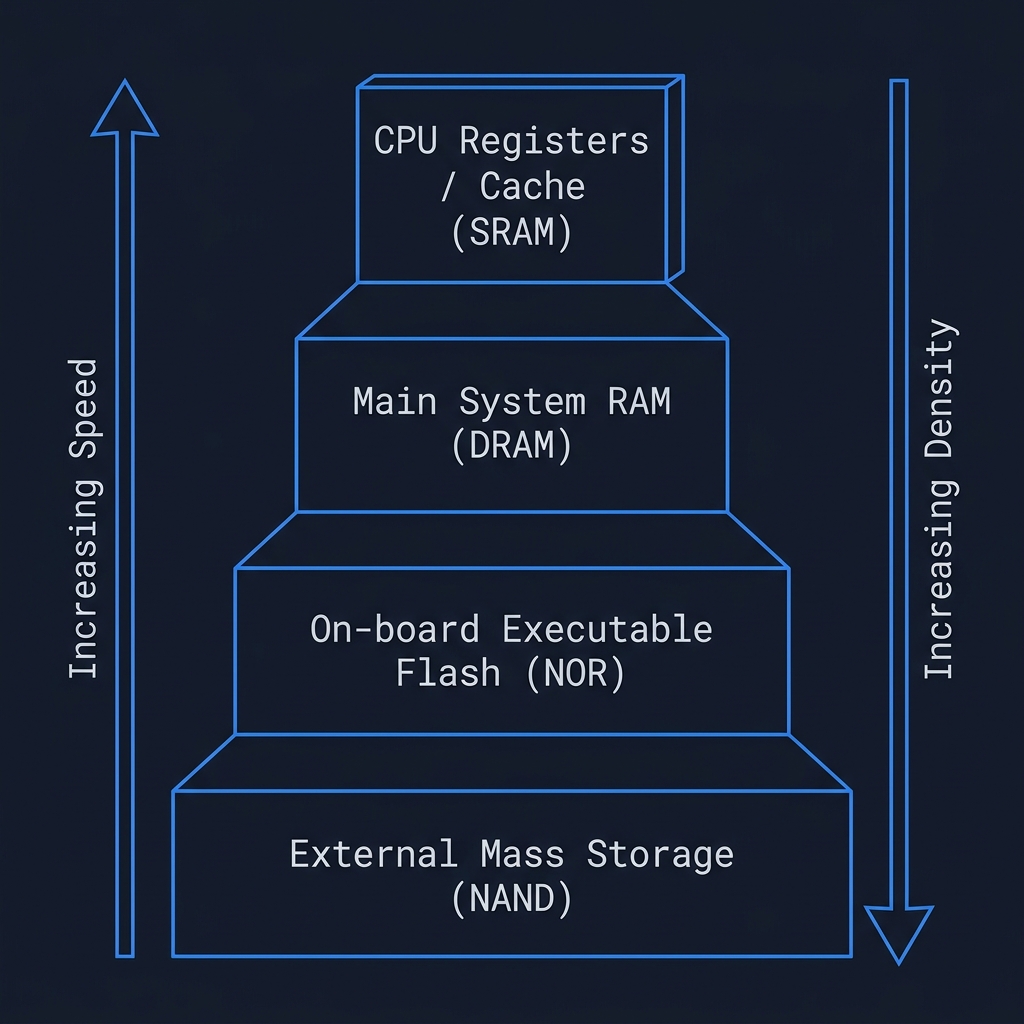
The Memory Hierarchy showing speed vs density trade-offs

A vertical structural view of memory layers tapering down as they approach the CPU core.

2. The Battle for the Bit: SRAM vs DRAM

At the volatile layer, the choice comes down to topology: how do we store a single bit of data?

Static RAM (SRAM) uses a cross-coupled latch constructed with 6 transistors (6T). This design creates an active, stable state that holds its value as long as power is applied. However, this complexity makes SRAM physically large and expensive, limiting its use to small, fast CPU caches and microcontroller registers.

Dynamic RAM (DRAM) takes the opposite approach. It shrinks the cell down to a single transistor and a single storage capacitor (1T1C). While this allows massive densities (gigabytes on a single chip), the capacitor is a leaky reservoir. It naturally drains its charge within milliseconds, requiring a continuous refresh loop to prevent data corruption.
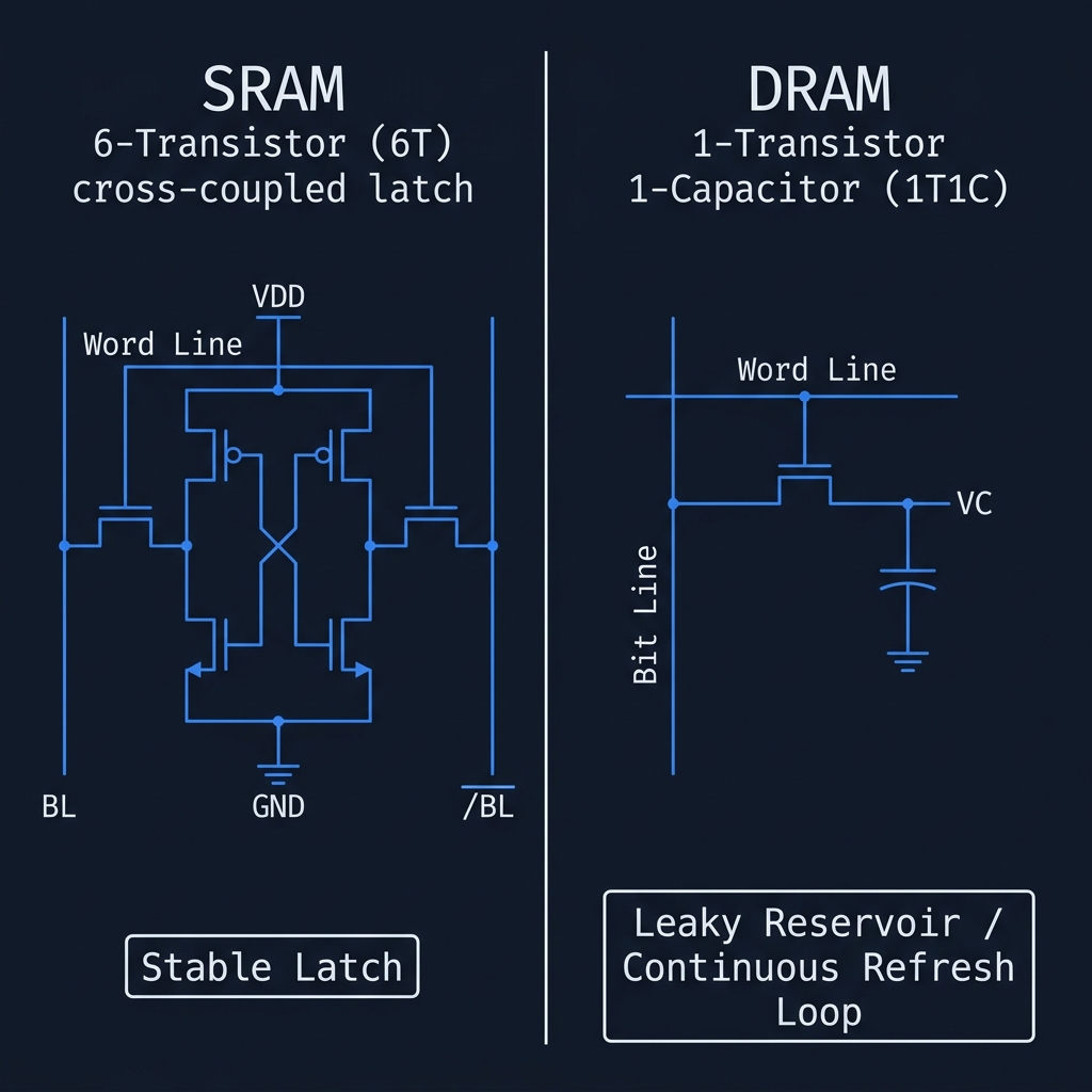
SRAM 6T vs DRAM 1T1C circuit diagram

Circuit topologies representing the active stable latch of SRAM versus the leaky reservoir of DRAM.

3. Persistence: NOR vs NAND Flash

When power is removed, we rely on non-volatile flash memory to retain our programs and data. Flash operates by trapping charge within a floating gate transistor. The layout configuration of these gates determines how they can be accessed.

NOR Flash connects storage transistors in parallel directly across word lines. This parallel alignment allows the processor to perform instant random byte reads, making it the standard choice for executing firmware binary code directly on-board.

NAND Flash daisy-chains transistor arrays in a tight serial configuration. By eliminating the individual contacts needed for parallel routing, NAND achieves extraordinary densities. However, this serial chain prevents byte-level access, requiring the processor to read and write data in sequential sector blocks, ideal for mass storage filesystems.
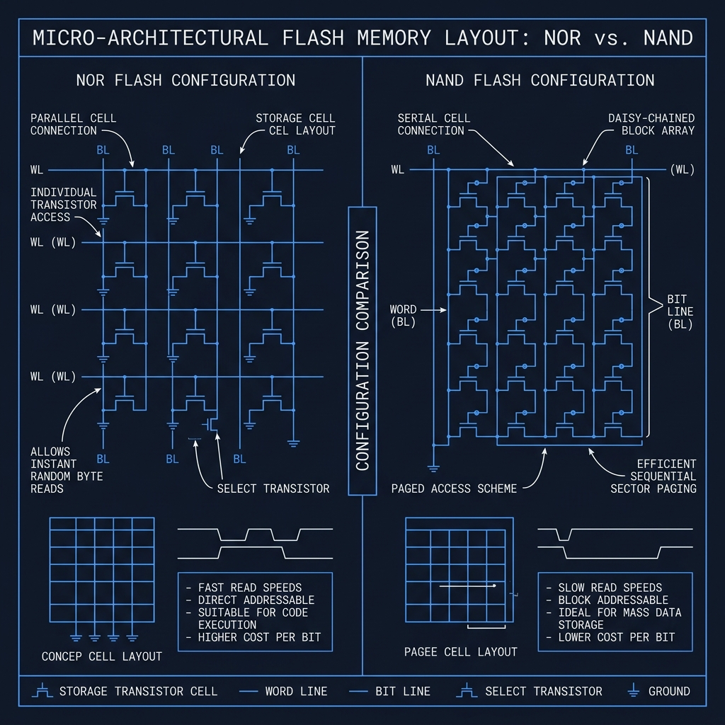
NOR parallel vs NAND serial micro-architectural layouts

Transistor cell layout detailing parallel random-access lines in NOR vs serial block lines in NAND.

4. The Address Map: Dividing Space

To the developer, all of these physical layers are abstracted into a single, contiguous address space. The microcontroller registers map specific memory regions to Flash and SRAM boundaries.

From top to bottom, the register space is divided into proportional segments: .text (NOR Flash for execution), .data and .bss (RAM for initialized and zeroed variables), followed by the Stack (runtime context engine) and the Heap (dynamic allocation workspace).
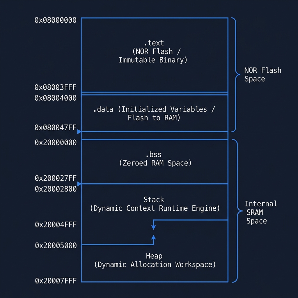
Microcontroller memory map segment boundaries

The vertical register allocation of persistent Flash versus internal SRAM workspace segments.

The Architecture of State

Memory is not just a passive buffer; it is the physical medium where logic meets reality. The boundaries of digital state are defined by the speeds, densities, and physical layout structures of silicon.

Understanding these hardware constraints is what allows us to write firmware that pushes performance to the very edge.

True efficiency is achieved when you align your software execution path with the physical layout of the silicon.
System Tree Node Computation
ABOUT PRAJNAEDGE

Engineering concepts you don't just read — you experience.

PrajnaEdge is an interactive engineering platform where complex concepts become experiences—through visual explorations, simulations, and practical understanding.

WHY PRAJNAEDGE EXISTS

Engineering is often taught as a collection of isolated concepts.

A processor here.
A protocol there.
An operating system somewhere else.

But real systems are built by connecting these layers.

PrajnaEdge exists to make those connections visible.

Each exploration starts with a question, builds an intuition, and gradually reveals the system underneath through visualizations, simulations, practical scenarios, and connections between concepts.

HOW PRAJNAEDGE WORKS

PrajnaEdge is designed around exploration rather than passive reading.

Concepts are introduced progressively, visualized when they benefit from seeing them, and brought to life through interactive EdgeCases and simulations where appropriate.

The goal is not simply to explain what a system does, but to help the learner understand why it works the way it does.

CREATOR PROFILE

Devaharsha Meesarapu

Embedded Systems • Firmware • Edge AI

I am the engineer behind the design, development, and content of PrajnaEdge. I build low-level systems where code directly controls hardware, bridging the gap between register-level silicon behavior and intelligent edge decision loops.

View Resume →

ABOUT ME

I am an Embedded Firmware Engineer focused on developing software for resource-constrained systems. My experience spans bare-metal firmware, device drivers, microcontroller peripherals, and communication protocols, working across the boundary between hardware and software.

My work has involved microcontroller-based systems, real-time behaviour, hardware interfaces, and communication technologies such as CAN, CAN FD, UART, SPI, and I²C. I am particularly interested in understanding systems from the lowest level upward—from registers and peripherals to intelligent edge systems.

ENGINEERING PHILOSOPHY

Engineering is not just about writing code; it is about managing constraints, timings, and physical hardware characteristics. True mastery of complex systems comes from understanding the interactions across different layers of the stack.

This conviction is why I built PrajnaEdge—to bridge the gap between conceptual theory and direct, register-level physical reality.

CONNECT

LinkedIn → GitHub →

Interactive Career Journey

Let's Connect
Interested in embedded systems, AI, or building something meaningful? I'd love to hear from you.
Open to collaborations, research, and interesting engineering conversations.
Help Improve PrajnaEdge
Found something to improve? I'd love to hear your thoughts.

Bare Metal

Software that runs directly on hardware without an operating system.

Applications
Operating Systems
YOU ARE HERE
Bare Metal
Processor
Hardware

"Every embedded application begins long before main()."

Operating Systems

An Operating System manages hardware and software resources so complex applications can work efficiently.

Applications
YOU ARE HERE
Operating Systems
Bare Metal
Processor
Hardware

"When one loop is no longer enough to carry the burden."

Support PrajnaEdge

PrajnaEdge is an independent education platform built to make knowledge freely accessible.

If you find PrajnaEdge useful, you can support its continued development.

Your support helps fund the time, tools, infrastructure, and experimentation that go into building and maintaining PrajnaEdge.

Select Region
Select Amount
Select an amount to support PrajnaEdge.